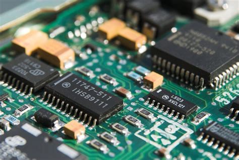
10 Essential Tips to Ensure PCB Assembly Success
Printed Circuit Board (PCB) assembly is a critical process in electronics manufacturing, where components are mounted onto a PCB to create a functional circuit. A successful PCB assembly ensures reliability, performance, and longevity of the final product. However, even minor errors can lead to failures, delays, and increased costs.
To help you achieve a smooth and successful PCB assembly process, here are 10 essential tips to follow:
1. Design for Manufacturability (DFM)
Before sending your PCB design for assembly, ensure it follows Design for Manufacturability (DFM) principles. DFM checks help identify potential manufacturing issues early, such as:
- Incorrect pad sizes for components
- Insufficient spacing between traces and components
- Missing solder mask between pads
- Improperly placed vias
Using DFM tools or consulting with your manufacturer can prevent costly redesigns and assembly errors.
2. Choose the Right PCB Manufacturer
Selecting a reliable PCB assembly manufacturer is crucial. Consider the following when choosing a partner:
- Experience in handling similar PCB types (rigid, flex, HDI, etc.)
- Certifications (ISO, IPC standards)
- Turnaround time and scalability
- Testing and quality control processes
A trusted manufacturer will help optimize your design and reduce assembly risks.
3. Accurate Bill of Materials (BOM)
A well-prepared Bill of Materials (BOM) is essential for PCB assembly success. Ensure your BOM includes:
- Correct part numbers (MPN or SKU)
- Manufacturer names (for critical components)
- Alternate part options (in case of shortages)
- Footprint and package details
An inaccurate BOM can lead to wrong components being placed, causing delays and rework.
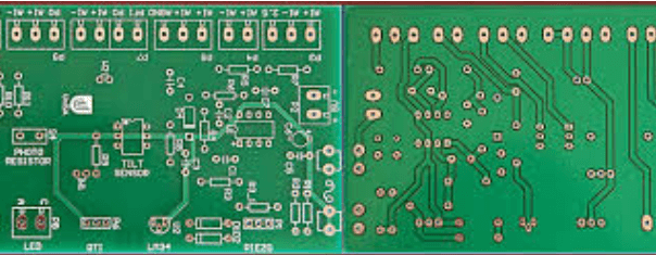
4. Optimize Component Placement
Proper component placement affects assembly yield and PCB performance. Follow these guidelines:
- Avoid placing small components near large ones (prevents shadowing during soldering)
- Ensure proper spacing for automated pick-and-place machines
- Orient polarized components uniformly (eases inspection)
- Place test points strategically for easier debugging
A well-optimized layout improves soldering quality and reduces defects.
5. Select the Right Soldering Technique
Choosing the correct soldering method is critical for reliable PCB assembly:
- Reflow Soldering: Best for surface-mount devices (SMDs)
- Wave Soldering: Ideal for through-hole components
- Selective Soldering: Used for mixed-technology boards
- Hand Soldering: For prototypes or rework
Using the wrong technique can lead to cold joints, bridging, or tombstoning.
6. Implement Proper Thermal Management
Excessive heat during assembly can damage components. To prevent thermal issues:
- Use a suitable solder profile (preheat, soak, reflow, cooling)
- Avoid overheating heat-sensitive components (e.g., LEDs, connectors)
- Ensure even heat distribution across the PCB
A well-controlled soldering process minimizes thermal stress and improves reliability.
7. Conduct Thorough Inspection and Testing
Post-assembly inspection and testing are vital for quality assurance:
- Automated Optical Inspection (AOI): Detects soldering defects
- X-ray Inspection: Checks hidden solder joints (e.g., BGA components)
- In-Circuit Testing (ICT): Verifies electrical functionality
- Functional Testing: Ensures the PCB works as intended
Skipping inspections increases the risk of undetected failures.
8. Manage Moisture-Sensitive Components
Many components (e.g., ICs, BGAs) are moisture-sensitive and can be damaged if not stored properly. Follow these steps:
- Store components in moisture-proof bags with desiccants
- Bake components before assembly if exposed to humidity
- Follow IPC/JEDEC J-STD-033 standards for handling
Neglecting moisture control can lead to popcorning (internal cracks) during soldering.
9. Ensure Proper Stencil Design for Solder Paste
A well-designed solder paste stencil ensures precise deposition and prevents defects:
- Aperture size and shape should match component pads
- Stencil thickness affects paste volume (typically 0.1mm–0.15mm for SMDs)
- Use nano-coating to improve paste release
A poorly designed stencil can cause solder bridging, insufficient solder, or tombstoning.
10. Plan for Rework and Debugging
Even with careful planning, some PCBs may need rework. Prepare by:
- Including test points for debugging
- Keeping spare components for replacements
- Documenting assembly issues for future improvements
Having a rework strategy minimizes downtime and improves yield.
Conclusion
Successful PCB assembly requires attention to detail at every stage—from design to testing. By following these 10 essential tips, you can minimize errors, improve quality, and ensure a smooth manufacturing process. Partnering with an experienced PCB assembly provider, maintaining accurate documentation, and implementing rigorous testing will help deliver reliable, high-performance PCBs.
By adhering to these best practices, you can reduce costs, speed up production, and achieve consistent PCB assembly success.