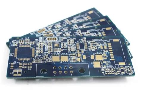
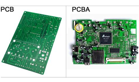
10 Golden Rules of PCB Layout, Routing, and Design Manufacturing
Printed Circuit Board (PCB) design is a critical aspect of electronics engineering, influencing performance, reliability, and manufacturability. A well-designed PCB ensures signal integrity, reduces electromagnetic interference (EMI), and simplifies assembly. Below are 10 golden rules to follow for optimal PCB layout, routing, and manufacturing.
1. Plan the Schematic Before Layout
A well-organized schematic is the foundation of a good PCB design. Before starting the layout:
- Label components clearly to avoid confusion.
- Group related circuits (e.g., power supply, analog, digital) for easier routing.
- Verify net connections to prevent errors in the layout phase.
A clean schematic ensures a smoother transition to PCB design and reduces debugging time.
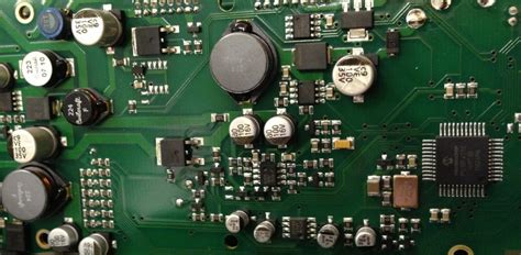
2. Optimize Component Placement
Proper component placement affects signal integrity, thermal management, and manufacturability. Follow these guidelines:
- Place critical components first (e.g., microcontrollers, FPGAs, sensors).
- Group related components (e.g., decoupling capacitors near IC power pins).
- Consider mechanical constraints (connectors, mounting holes).
- Minimize trace lengths to reduce parasitic inductance and resistance.
Good placement reduces routing complexity and improves performance.
3. Follow a Logical Routing Hierarchy
Routing should follow a structured approach:
- Power and ground traces – Ensure low impedance paths.
- Critical signals (high-speed, clock, differential pairs) – Route these first to avoid interference.
- General signal traces – Route remaining connections while avoiding crosstalk.
This hierarchy prevents signal integrity issues and simplifies troubleshooting.
4. Maintain Proper Trace Width and Spacing
Trace width and spacing impact current handling, impedance, and EMI:
- Power traces should be wider (e.g., 20-50 mils for high current).
- Signal traces can be narrower (e.g., 5-10 mils) but must match impedance requirements.
- Follow the 3W rule (keep traces 3x the width apart) to minimize crosstalk.
Manufacturing Design Rule Checks (DRC) should enforce these constraints.
5. Implement a Solid Grounding Strategy
A poor ground plane leads to noise and EMI issues. Best practices include:
- Use a continuous ground plane (avoid splits under high-speed signals).
- Separate analog and digital grounds (connect at a single point if needed).
- Minimize ground loops by keeping return paths short.
A well-designed ground system improves signal integrity and reduces noise.
6. Control Impedance for High-Speed Signals
High-speed signals (e.g., USB, HDMI, DDR) require controlled impedance:
- Match trace width and dielectric thickness to target impedance (e.g., 50Ω, 100Ω differential).
- Avoid sharp bends (use 45° or curved traces).
- Keep differential pairs tightly coupled with equal lengths.
Impedance mismatches cause signal reflections and degrade performance.
7. Minimize EMI and Crosstalk
Electromagnetic interference (EMI) can disrupt circuit operation. Mitigation techniques include:
- Separate high-speed and sensitive analog signals.
- Use guard traces or ground shielding near noisy lines.
- Avoid parallel routing of high-speed traces over long distances.
- Add ferrite beads or filters for noise suppression.
Proper EMI management ensures compliance with regulatory standards (FCC, CE).
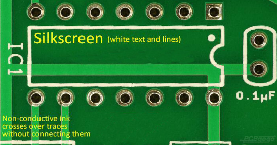
8. Optimize Power Distribution
A stable power supply is crucial for reliable operation:
- Use multiple vias for power and ground connections to reduce inductance.
- Place decoupling capacitors close to IC power pins (e.g., 0.1µF for high-frequency noise).
- Implement power planes for low-impedance distribution.
Poor power distribution can lead to voltage drops and erratic behavior.
9. Design for Manufacturability (DFM)
A PCB must be easy to manufacture and assemble:
- Follow manufacturer’s design rules (minimum trace width, hole sizes, spacing).
- Avoid acute angles in traces (can cause etching issues).
- Include fiducial marks for automated assembly.
- Test points should be accessible for debugging.
DFM reduces production costs and improves yield.
10. Perform Design Verification Before Production
Before sending a PCB for fabrication:
- Run Design Rule Check (DRC) to catch errors.
- Verify signal integrity with simulations (if applicable).
- Check for thermal hotspots (especially in power circuits).
- Review assembly drawings to ensure correct component placement.
A thorough review prevents costly redesigns and delays.
Conclusion
Following these 10 golden rules ensures a robust, high-performance PCB design that is manufacturable and reliable. By focusing on proper planning, routing strategies, grounding, EMI control, and DFM, engineers can avoid common pitfalls and deliver professional-grade PCBs.
Whether designing a simple microcontroller board or a complex high-speed system, adhering to these principles will lead to better functionality, lower costs, and faster time-to-market.