20 questions about very practical high-frequency PCB circuit design
1.How to choose PCB board materials?
When choosing PCB board materials, a balance must be struck between meeting design requirements, mass production and cost. Design requirements include electrical and mechanical parts. Usually, when designing very high-speed PCB boards (frequencies greater than GHz), this material issue is more important. For example, in the commonly used FR-4 material, the dielectric loss at a frequency of several GHz will have a great impact on signal attenuation, and it may not be applicable. As for electrical, pay attention to whether the dielectric constant and dielectric loss are suitable for the designed frequency.
2.How to avoid high-frequency interference?
The basic idea of avoiding high-frequency interference is to minimize the interference of the electromagnetic field of high-frequency signals, which is also called crosstalk. You can increase the distance between high-speed signals and analog signals, or add ground guard/shunt traces next to analog signals. You must also pay attention to the noise interference of digital ground to analog ground.
3.In high-speed design, how to solve the problem of signal integrity?
Signal integrity is basically an impedance matching problem. Factors that affect impedance matching include the architecture of the signal source and the output impedance, the characteristic impedance of the routing, the characteristics of the load end, and the topology of the routing. The solution is to rely on termination and adjust the topology of the routing.
4.How is the differential routing method implemented?
There are two points to note in the wiring of differential pairs. One is that the length of the two lines should be as equal as possible, and the other is that the spacing between the two lines (this spacing is determined by the differential impedance) should always remain unchanged, that is, to keep them parallel. There are two ways to parallelize. One is that the two lines are on the same routing layer (side-by-side), and the other is that the two lines are on the upper and lower adjacent layers (over-under). Generally, the former side-by-side is more often implemented.
5.How to realize differential wiring for clock signal lines with only one output?
When differential wiring is used, it must be meaningful only when the signal source and the receiving end are also differential signals. Therefore, differential wiring cannot be used for clock signals with only one output.
6.Can a matching resistor be added between the differential line pairs at the receiving end?
Matching resistors between differential line pairs at the receiving end are usually added, and their values should be equal to the value of differential impedance. In this way, the signal quality will be better.
7.Why should the wiring of differential pairs be close and parallel?
The wiring method for differential pairs should be appropriately close and parallel. The so-called appropriate closeness is because the spacing will affect the value of differential impedance, and this value is an important parameter for designing differential pairs. Parallel is also required because the consistency of differential impedance must be maintained. If the two lines are sometimes far and sometimes close, the differential impedance will be inconsistent, which will affect signal integrity and timing delay.
8.How to deal with some theoretical conflicts in actual wiring
Basically, it is right to separate the analog/digital ground. It should be noted that the signal routing should not cross the split place (moat) as much as possible, and the returning current path of the power supply and signal should not be too large.
The crystal oscillator is an analog positive feedback oscillation circuit. To have a stable oscillation signal, the loop gain and phase specifications must be met. However, the oscillation specification of the analog signal is easily interfered with. Even if ground guard traces are added, it may not be possible to completely isolate the interference. Moreover, if it is too far away, the noise on the ground plane will also affect the positive feedback oscillation circuit. Therefore, the distance between the crystal oscillator and the chip must be as close as possible.
It is true that there are many conflicts between high-speed wiring and EMI requirements. But the basic principle is that the resistors, capacitors or ferrite beads added due to EMI cannot cause some electrical characteristics of the signal to not meet the specifications. Therefore, it is best to use the techniques of arranging routing and PCB stacking to solve or reduce EMI problems, such as routing high-speed signals on the inner layer. Finally, resistors, capacitors or ferrite beads are used to reduce the damage to the signal.
9.How to solve the contradiction between manual routing and automatic routing of high-speed signals?
Most of the current powerful routing software automatic routing devices have set constraints to control the winding method and the number of vias. The winding engine capabilities and constraint setting items of various EDA companies are sometimes very different. For example, whether there are enough constraints to control the winding method of the serpentine, whether the routing spacing of the differential pair can be controlled, etc. This will affect whether the routing method generated by automatic routing can meet the designer’s ideas. In addition, the difficulty of manually adjusting the routing is also absolutely related to the ability of the winding engine. For example, the pushing ability of the routing, the pushing ability of the via, and even the pushing ability of the routing to the copper plating, etc. Therefore, choosing a routing device with a strong winding engine capability is the solution.
10.About test coupon.
The test coupon is used to measure the characteristic impedance of the produced PCB board with TDR (Time Domain Reflectometer) to see if it meets the design requirements. Generally, the impedance to be controlled is single line and differential pair. Therefore, the line width and line spacing (when there is a differential pair) on the test coupon should be the same as the line to be controlled. The most important thing is the location of the ground point during measurement. In order to reduce the inductance of the ground lead, the grounding point of the TDR probe is usually very close to the probe tip, so the distance and method between the point where the signal is measured on the test coupon and the grounding point should be consistent with the probe used.
11.In high-speed PCB design, the blank area of the signal layer can be copper-plated, and how should the copper of multiple signal layers be distributed in grounding and power supply?
Generally, the copper plating in the blank area is grounded in most cases. It is just that when plating copper next to the high-speed signal line, pay attention to the distance between the copper plating and the signal line, because the copper plating will reduce the characteristic impedance of the line a little. Also be careful not to affect the characteristic impedance of other layers, such as in the dual strip line structure.
12.Can the signal line on the power plane be calculated using the microstrip line model? Can the signal between the power and ground planes be calculated using the stripline model?
Yes, both the power plane and the ground plane must be considered as reference planes when calculating the characteristic impedance. For example, a four-layer board: top layer-power layer-ground layer-bottom layer. At this time, the model of the characteristic impedance of the top layer routing is a microstrip line model with the power plane as the reference plane.
13.Can the automatic generation of test points on high-density printed circuit boards by software generally meet the test requirements of mass production?
Whether the test points automatically generated by general software meet the test requirements depends on whether the specifications for adding test points meet the requirements of the test equipment. In addition, if the routing is too dense and the specifications for adding test points are strict, it may not be possible to automatically add test points to each line. Of course, the places to be tested need to be filled manually.
14.Will adding test points affect the quality of high-speed signals?
Whether it will affect the signal quality depends on the way of adding test points and how fast the signal is. Basically, the additional test point (without using the existing via or DIP pin as the test point) may be added to the line or a short line may be pulled out from the line. The former is equivalent to adding a very small capacitor to the line, and the latter is an additional branch. Both situations will have some impact on the high-speed signal, and the degree of impact is related to the frequency speed of the signal and the edge rate of the signal. The magnitude of the impact can be known through simulation. In principle, the smaller the test point, the better (of course, it must meet the requirements of the test equipment) and the shorter the branch, the better.
15.How should the ground wires between the boards of a system be connected when several PCBs are connected?
When the signals or power supplies between the interconnected PCB boards are in action, for example, when the power supply or signal from board A is sent to board B, there must be an equal amount of current flowing back from the ground to board A (this is Kirchoff current law). The current on the ground will flow back to the place with the smallest impedance. Therefore, at each interface where power or signal is connected to each other, the number of pins allocated to the ground layer cannot be too small to reduce impedance, which can reduce noise on the ground layer. In addition, the entire current loop can be analyzed, especially the part with larger current, and the connection method of the ground layer or ground wire can be adjusted to control the flow of current (for example, create low impedance at a certain place to let most of the current flow from this place) to reduce the impact on other more sensitive signals.
16.Can you introduce some foreign technical books and data on high-speed PCB design?
Now the application of high-speed digital circuits includes communication networks and calculators and other related fields. In the communication network, the operating frequency of PCB boards has reached around GHz, and the number of layers is as many as 40 as far as I know. Because of the progress of chips, the highest operating frequency on the board of computer-related applications has reached 400MHz (such as Rambus) or above, whether it is a general PC or server. In response to the demand for high-speed and high-density routing, the demand for blind/buried vias, mircrovias and build-up process technology is gradually increasing. These design requirements can be mass-produced by manufacturers.
17.Two commonly referenced characteristic impedance formulas:
Microstrip Z={87/[sqrt(Er+1.41)]}ln[5.98H/(0.8W+T)] Where W is the line width, T is the copper thickness of the routing, H is the distance from the routing to the reference plane, and Er is the dielectric constant of the PCB material. This formula must be applied when 0.1<(W/H)<2.0 and 1<(Er)<15.
Stripline Z=[60/sqrt(Er)]ln{4H/[0.67π(T+0.8W)]} Where H is the distance between the two reference planes, and the trace is located in the middle of the two reference planes. This formula can only be applied when W/H<0.35 and T/H<0.25.
18.Can a ground line be added in the middle of the differential signal line?
Generally, a ground line cannot be added in the middle of the differential signal. Because the most important point of the application principle of differential signals is to utilize the benefits brought by the mutual coupling (coupling) between differential signals, such as flux cancellation, noise immunity, etc. If a ground line is added in the middle, the coupling effect will be destroyed.
19.Does the design of rigid-flexible boards require special design software and specifications? Where can I undertake the processing of such circuit boards in China?
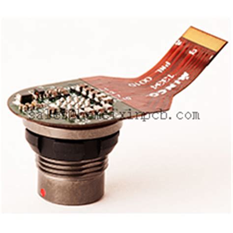
General PCB design software can be used to design flexible printed circuits (Flexible Printed Circuit). The same Gerber format is used for production by FPC manufacturers. Since the manufacturing process is different from that of general PCB, each manufacturer will have its own requirements for the minimum line width, minimum line spacing, and minimum aperture (via) based on their manufacturing capabilities. In addition, some copper foil can be laid at the turning point of the flexible circuit board for reinforcement. As for the manufacturer, you can search for “FPC” as a keyword on the Internet and you should be able to find it.
20.What is the principle for properly selecting the grounding points of the PCB and the shell?
The principle for selecting the grounding points of the PCB and the shell is to use the chassis ground to provide a low-impedance path for the returning current and control the path of this returning current. For example, usually near high-frequency devices or clock generators, the PCB ground layer and the chassis ground can be connected by fixing screws to minimize the area of the entire current loop, that is, to reduce electromagnetic radiation.

