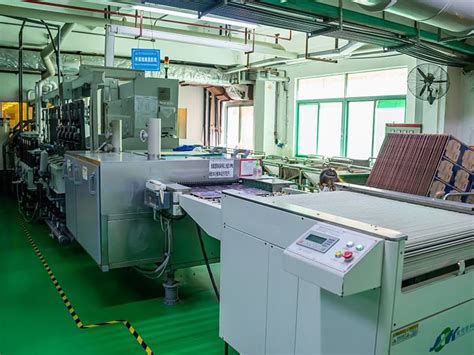
4 pcb assembly
What are the processes and advantages of 4 PCB assembly?
So how are 4 PCBs assembled? Let’s look at the PCB assembly process:
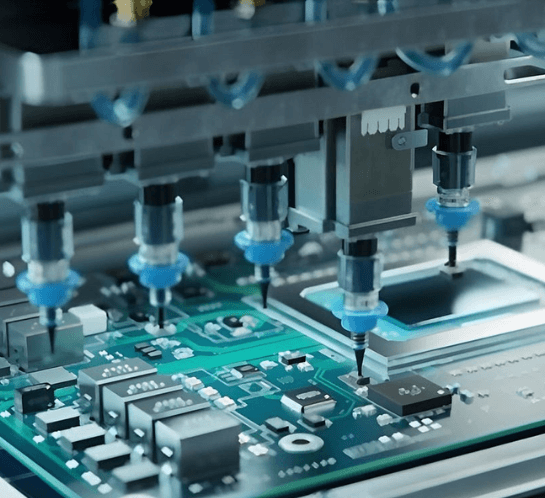
- Application of solder paste: First, solder paste (a small particle of solder paste mixed with flux) is applied to the board. For this application, most PCB manufacturers use stencils (available in several sizes, shapes, and specifications that match the specifications) that can only correctly apply the correct amount of solder paste to certain parts of the board.
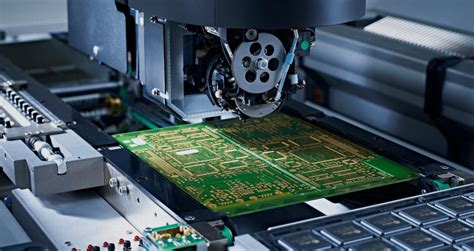
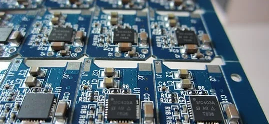
- Placement of components: Unlike in the past, this stage of the 4 PCB assembly process is now fully automated. The picking and placement of parts (such as surface mount components) was once done manually and is now performed by robotic pick and place machines.
These machines place components accurately to pre-planned areas of the circuit board. - Reflow: With the solder paste and all surface mount components in place, curing the solder paste to the correct specifications is essential for the PCB components to adhere properly to them.
This is the relevant part of this PCB assembly process – reflow soldering. To do this, the components with solder paste and the components on them are passed through a conveyor belt, which passes through an industrial-grade reflow oven.
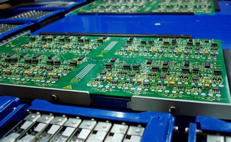
The heaters in the oven melt the solder in the solder paste. Once the melting is complete, the components are moved again in the conveyor belt and exposed to a series of cooler heaters. The purpose of these coolers is to cool the melted solder and allow it to solidify. - Inspection: After the reflow process, the PCB should be inspected to check its functionality. This stage helps identify poor quality connections, misplaced components, and short circuits caused by the continuous movement of the board during the reflow process.
PCB manufacturers employ multiple inspection steps such as manual inspection, automated optical inspection, and X-ray inspection to check the functionality of the board, identify lower quality solder, and find out any potential hidden dangers.
Once the inspection is completed, the assembly team makes a crucial decision. Boards with several functional errors are usually scrapped, on the other hand, if there are minor errors, the board is sent again for rework. - Through-hole component insertion: Some types of PCBs require the insertion of through-hole components along with regular SMD components.
This stage is dedicated to the insertion of such components. For this purpose, plated through holes are created with the help of which PCB components pass the signal from one side of the board to the other.
PCB through-hole insertion usually utilizes manual or wave soldering to obtain results. - Final Inspection: Now it is time for the second level inspection. Here, the assembled board is tested for functionality, or the PCB is thoroughly inspected to monitor its electrical characteristics, including voltage, current, or signal output.
Today’s manufacturers utilize a variety of advanced testing equipment to help determine the success or failure of the finished board. - Cleaning: Since the soldering process can leave a lot of flux residue in the PCB, it is crucial to thoroughly clean the assembly before the final circuit board is delivered to the customer. To do this, the PCBs are cleaned in deionized water. After the cleaning process, the board is thoroughly dried using compressed air. The PCB assembly is now ready for customer inspection.
What are the advantages of 4 PCB assembly?
For businesses of all sizes, there are several significant advantages to 4 PCB assembly.
After all the conveniences of outsourcing, a critical part that enables the product to run smoothly is considerable.
However, when it comes to startups and small businesses, the advantages that come with choosing a turnkey PCB supplier can have a significant strategic impact on the business.
Before considering some of the advantages, it would be worthwhile to define what full PCB assembly actually means. In short, PCB assembly means that the PCB supplier takes care of every aspect of the PCB project.
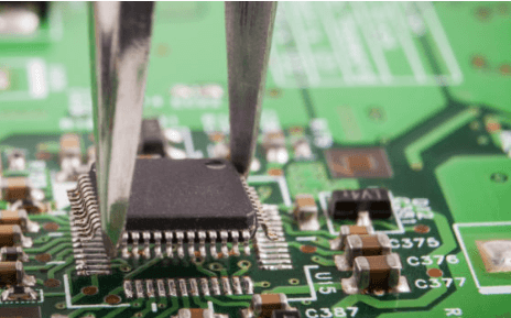
This means sourcing components, manufacturing, and assembly. Here are some of the key advantages that small businesses can benefit from:
- Save time
With a turnkey manufacturer handling the entire PCB assembly, the obvious advantage that accumulates is saving the client team valuable time to focus on other aspects of the business, which is where their expertise lies.
As a customer, you don’t need to spend time and energy looking for cost-effective quotes for individual components, go through the hassle of sourcing them, and then put all these quotes together. This works well from a cost perspective as well, as turnkey services are priced far more effectively than bundled services.
- Helps you identify problems at the outset
The main advantage that arises when going with turnkey PCB assembly at the prototype stage is also the ability to identify any problems early on. In fact, once you share the netlist file with the turnkey manufacturer, he will be able to point out errors, if any.
These errors can then be corrected on their own during the design phase, rather than making costly changes once you are ready to go through full production, or worse, when you have already completed production and need to make changes.
- Better management
The full PCB assembly advantage also lies in the fact that you don’t have to deal with multiple suppliers. This has many other advantages besides saving time. What you also save is the miscommunication that can occur when dealing with multiple suppliers.
With a turnkey supplier, you may have only one point of contact, which makes the process seamless. Since delivery schedules are critical, the slightest misunderstanding between suppliers can cause the entire schedule to go wrong and lead to costly consequences. With a turnkey supplier, you can rest assured that the entire responsibility for timely delivery lies with them.
- Other services
Turnkey suppliers also often provide other services, including inventory and sales. Shipping and so on. For small businesses and startups, the importance of these services cannot be underestimated because you don’t have to spend time, energy and manpower on these aspects, and you can control costs, giving you a competitive advantage.
Look at the current commercial use of PCBA, it is like the hub of various smart appliances, without which these appliances will not work. Since the development direction of PCBA is to be applied to smart electronic products, it must keep pace with the times, which requires the continuous infiltration of high-tech research and development. Without a good R&D team, it is impossible to do this well.
Shenzhen Kuaifa Intelligent Manufacturing Co., Ltd. is a one-stop service provider focusing on intelligent manufacturing of PCBA and finished product assembly of various mid-to-high-end electronic products such as industrial automation, automotive electronics, medical electronics, power electronics, etc. It has a team of more than 30 experienced R&D engineers and has the design and development capabilities of artificial intelligence products and smart small household appliances. The company provides customers with diversified PCBA, finished product development and manufacturing services in a high-quality, efficient and fast way, and can provide small and medium-sized batch production. It is your trusted partner!
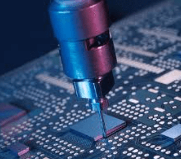
Technical points of 4 pcb assembly
- Design stage
(1) Layout planning: According to the functional requirements of the circuit, rationally plan the layout of components to ensure smooth signal transmission and reduce interference.
(2) Wiring design: Adopt reasonable wiring strategies, such as differential pair wiring, ground wire wrapping, etc., to improve signal integrity and stability.
(3) Power and ground wire design: Rationally distribute power and ground wires to ensure the stability and reliability of the circuit board. - Material selection stage
(1) Substrate material selection: Select appropriate substrate materials according to product requirements, such as FR4, CEM-1, etc.
(2) Component selection: Select appropriate components according to circuit design and performance requirements to ensure component quality and reliability. - Wiring stage
(1) Top and bottom layer wiring: The top and bottom layers are wired according to design requirements, paying attention to avoid signal interference and crossover.
(2) Middle layer wiring: Wiring the power and ground wires in the middle layer to ensure balanced and stable power distribution.
(3) Through hole, blind hole and buried hole processing: Use through hole, blind hole and buried hole and other connection methods as needed to improve the connection performance and reliability of the circuit board. - Welding and assembly stage
(1) Welding process selection: Select the appropriate welding process according to the component type and size, such as wave soldering, reflow soldering, etc.
(2) Welding quality control: Ensure welding quality and avoid welding defects such as cold soldering and short circuit.
(3) Assembly and debugging: Assemble and debug the components according to the design requirements to ensure that the function and performance of the circuit board meet the requirements. - Testing and inspection stage
(1) Functional test: Perform functional test on the circuit board to ensure that each functional module works normally.
(2) Performance test: Perform performance test on the circuit board, such as electrical performance, thermal performance, etc., to ensure that the circuit board meets the design requirements.
(3) Reliability test: Perform reliability test on the circuit board, such as performance test under high temperature, low temperature, vibration and other environmental conditions to ensure the stability and reliability of the circuit board.

