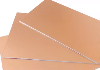
5 copper
5 Copper PCB (Printed Circuit Board) plays a vital role in modern electronic devices. Its manufacturing process and application range are wide and worth in-depth discussion. First of all, the manufacturing process of 5 copper PCB is complex and delicate, involving multiple key steps.
1.the manufacturing process starts with the selection of substrates.
.Commonly used substrates include FR-4, CEM-1, etc. These materials have good insulation properties and mechanical strength. Next, a uniform layer of copper foil is formed on the surface of the substrate through chemical deposition or electroplating process. This process ensures the conductivity of the circuit board.
2.pattern transfer
After the copper foil is formed, the next step is pattern transfer, that is, transferring the designed circuit pattern to the copper foil. Photolithography technology is usually used to accurately transfer the circuit pattern to the 5 copper foil through photosensitive materials and ultraviolet exposure. Subsequently, the excess copper foil is removed by etching process, leaving only the required circuit pattern. The accuracy of the etching process directly affects the performance of the circuit board, so the etching time and solution concentration need to be strictly controlled.
3.the circuit board needs to be drilled and electroplated
After etching, the circuit board needs to be drilled and electroplated to install electronic components and realize the interconnection of multi-layer circuits. The drilling process usually uses a high-precision CNC drilling machine to ensure the accuracy of the aperture and position. The electroplating process forms a conductive channel by depositing a layer of copper on the hole wall, thereby achieving electrical connection between different layers. Finally, the surface of the circuit board needs to be protected, such as coating a solder mask and silk-screening logo, to improve the durability and maintainability of the circuit board.

5 Copper PCBs have a wide range of applications, covering almost all electronic devices. From consumer electronics such as smartphones and tablets to industrial control equipment and automotive electronics, copper PCBs are indispensable core components. Its excellent electrical and thermal conductivity make it particularly outstanding in high-frequency and high-speed circuits. In addition, copper PCBs are also widely used in power modules and LED lighting and other fields because they can effectively dissipate heat and ensure the stable operation of the equipment.
It is worth mentioning that with the continuous miniaturization and high performance of electronic equipment, the requirements for copper PCBs are also getting higher and higher. The development of high-density interconnect (HDI) technology, multi-layer board technology and flexible circuit board technology enables copper PCBs to meet more complex and higher-performance application requirements. For example, in 5G communication equipment, high-frequency and high-speed signal transmission has extremely high requirements for circuit boards. Copper PCBs have become the preferred material due to their excellent electrical performance and reliability.
In summary, the manufacturing process of copper PCB is delicate and complex, and its application range is wide and expanding. Its importance in modern electronic devices is self-evident, and with the continuous advancement of technology, copper PCB will continue to play a key role in the electronics industry.


