
50-Layer PCB Registration Accuracy: Manufacturing Tolerances Explained
Registration accuracy determines whether every layer in your 50-layer PCB aligns precisely during lamination. A misalignment of just 75μm (3 mils) can cause via breakouts, signal integrity failures, and scrapped boards worth thousands of dollars. In high layer count manufacturing, registration tolerances compound through sequential lamination cycles, making tolerance management the difference between a functional board and expensive rework.
What is PCB Registration Accuracy?
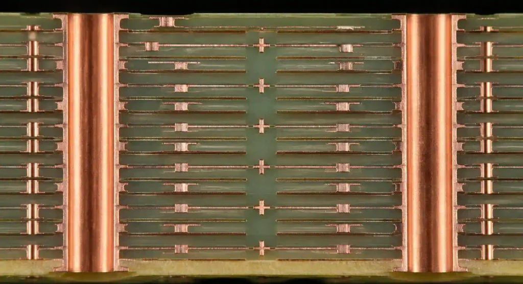
Registration accuracy measures how precisely inner layers align to each other and to the outer layers during lamination. Perfect registration means every drilled via lands exactly in the center of its target pad on every layer. Real manufacturing introduces xy-offset errors that accumulate as layer count increases.
For 50-layer PCBs, registration tolerances directly impact design rules. You must size capture pads large enough to accommodate worst-case misalignment while maintaining electrical performance. IPC-6012 Class 3 requires minimum 50μm (2 mils) annular ring after drilling—but that assumes you correctly calculated the registration tolerance budget first.
How Registration Errors Accumulate in Multilayer PCBs
Sequential Lamination and Tolerance Build-Up
Standard multilayer PCBs (4-16 layers) use single-shot lamination where all layers stack and press simultaneously. Registration error in this process is typically ±75μm (±3 mils) per IPC-6012 Class 2, or ±50μm (±2 mils) for Class 3.
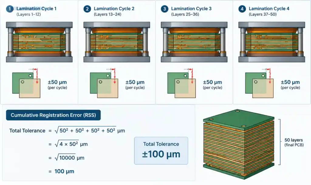
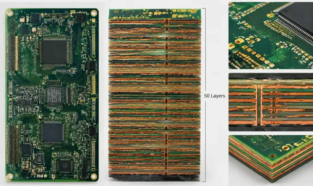
50-layer PCBs require sequential lamination—you cannot physically align 50 layers at once. Manufacturers build the stack in stages: core fabrication, sub-composite assembly, and final lamination. Each cycle introduces independent registration error that combines as root sum square (RSS), not simple addition.
Registration Tolerance Calculation
| Lamination Stage | Typical Tolerance (Class 3) | Cumulative RSS |
|---|---|---|
| Core layers (2-layer pairs) | ±50μm | ±50μm |
| First build-up (add 8 layers) | ±50μm | ±71μm |
| Second build-up (add 8 layers) | ±50μm | ±87μm |
| Final lamination (add outer layers) | ±50μm | ±100μm |
Formula: Total tolerance = √(T₁² + T₂² + T₃² + … + Tₙ²)
For four lamination cycles at ±50μm each: √(50² + 50² + 50² + 50²) = ±100μm total registration tolerance.
Inner Layer Alignment Methods
Optical Registration Systems
Modern PCB fabs use automated optical alignment that detects registration targets on each layer and adjusts xy-position before lamination. These systems achieve ±25μm alignment accuracy under controlled conditions.
Tooling holes serve as mechanical references, but optical targets provide the actual alignment data. Vision systems measure target position to sub-pixel accuracy (5-10μm resolution) and calculate required translation and rotation correction.
Key limitation: Optical systems align layers before pressing. Material movement during lamination—caused by resin flow, thermal expansion, and pressure gradients—introduces additional error that optical pre-alignment cannot predict.
Registration Targets Design
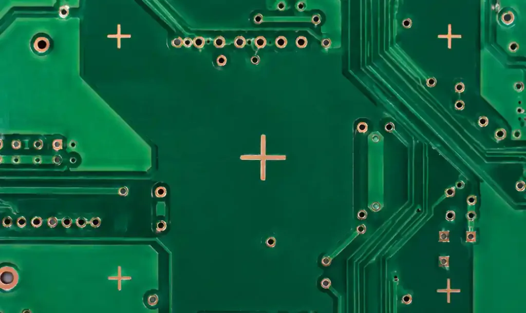
Effective registration targets must survive inner layer processing and remain detectable through prepreg:
- Solid copper crosses: 1mm × 1mm with 0.2mm line width
- Placement: Three non-collinear positions per panel
- Clearance: Minimum 10mm from panel edge
- Protection: Complete copper removal around targets for high contrast
Lamination Press Considerations
Thermal Expansion Effects
FR-4 has coefficient of thermal expansion (CTE) around 14-17 ppm/°C. For a 500mm panel heated from 25°C to 180°C during pressing:
ΔL = 500mm × 16 ppm/°C × 155°C = 1.24mm expansion
Layers aligned optically at room temperature shift position during the 180°C press cycle. This thermal-mechanical effect accounts for 30-50% of total registration error in sequential lamination.
Advanced manufacturers use CTE-matched prepreg systems and temperature-profiled pressing to minimize thermal movement.
Press Uniformity and Vacuum Lamination
Non-uniform pressure causes layers to slide during lamination. Resin flow from prepreg acts as a lubricant—if pressure gradients exist, layers can shift 25-50μm before curing.
| Press Type | Registration Performance | Application |
|---|---|---|
| Single-daylight hydraulic | ±75-100μm | Up to 20 layers |
| Multi-daylight with zone control | ±50-75μm | 20-40 layers |
| Vacuum-assisted lamination | ±50μm | 40+ layers |
Vacuum lamination evacuates air, eliminating voids and reducing resin-flow-induced shifting. This technology is essential for HDI PCB and 50-layer builds.

Via Capture Pad Sizing for Manufacturing Tolerances
Design Rule Calculation
Via capture pads must guarantee minimum annular ring after accounting for all tolerances:
Pad diameter = Drill diameter + 2 × (Min annular ring + Registration tolerance + Drill positioning + Plating variation)
For a 0.3mm (12 mil) drilled via in a 50-layer board:
- Drill diameter: 0.30mm
- Minimum annular ring (IPC-6012 Class 3): 0.05mm
- Registration tolerance (4 cycles): 0.10mm
- Drill positioning: 0.075mm
- Plating variation: 0.01mm
Calculated pad diameter = 0.30 + 2 × (0.05 + 0.10 + 0.075 + 0.01) = 0.77mm (30 mils)
This ensures no via breakout under worst-case tolerance stack-up.
Layer-Specific Pad Sizing
Some manufacturers vary capture pad size by layer depth:
- Outer layers (L1, L50): 0.65mm pads (better registration control)
- Near-surface (L2-L5, L46-L49): 0.70mm pads
- Core layers (L20-L30): 0.77mm pads (worst-case tolerance)
This saves board space on outer layers while providing adequate margin on buried layers.
Inspection Methods for Registration Accuracy
X-Ray and Optical Inspection
Automated optical inspection (AOI) measures registration after drilling by imaging via-to-pad alignment. X-ray inspection penetrates the stack to image buried vias.
3D X-ray laminography reconstructs individual layer images from multiple angles, accurately measuring registration on specific buried layers. This requires expensive equipment but provides non-destructive verification.
Microsectioning and Cross-Section Analysis
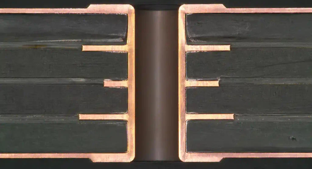
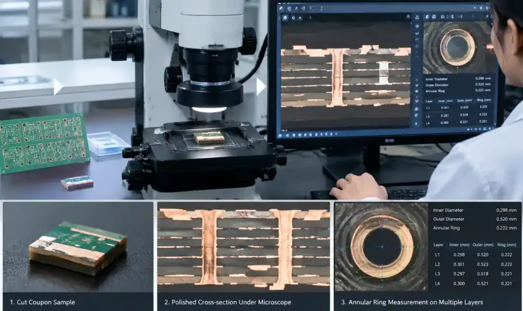
Destructive cross-sectioning remains the definitive verification method. The fab cuts coupons from panel corners, polishes to expose via cross-sections, and measures annular ring on each layer under microscopy.
IPC-6012 Class 3 requires minimum 50μm annular ring. If any layer shows less, the board fails. Expect 10-15 cross-section samples per lot during 50-layer qualification.
Achievable Tolerances in Modern Manufacturing
IPC Standards vs Real Capability
| IPC Class | Registration Tolerance | Application |
|---|---|---|
| Class 1 (General) | ±150μm (±6 mils) | Consumer electronics |
| Class 2 (Standard) | ±75μm (±3 mils) | Telecom, industrial |
| Class 3 (High Reliability) | ±50μm (±2 mils) | Aerospace, medical |
These are per-feature tolerances. For 50-layer sequential build-up, apply RSS calculation for total stack-up tolerance.
Real manufacturing capability:
- Standard process: ±75μm per cycle, ±130-150μm total
- Controlled process: ±50μm per cycle, ±100μm total (optical + vacuum)
- Advanced process: ±40μm per cycle, ±80μm total (adds CTE-matched materials)
Andwin Circuits achieves ±50μm per-cycle registration using automated optical alignment and multi-zone vacuum lamination. Our special PCB facility handles up to 50-layer boards with IPC-6012 Class 3 compliance.
Design for Manufacturing Guidelines
- Capture pad sizing: Use ±100μm registration tolerance in pad calculations
- Via placement: Avoid vias within 0.5mm of high-density BGA fields
- Test coupons: Include daisy-chain via structures for continuity verification
- Material selection: Specify low-CTE laminates (12-14 ppm/°C)
- Supplier qualification: Request registration capability data from prior 40+ layer builds
Our PCB manufacturing process includes first-article cross-sectioning for all 40+ layer orders.
Registration Impact on Electrical Performance
Via breakouts and minimal annular rings increase via inductance but cause no measurable electrical difference above 50μm annular ring at frequencies below 10 GHz.
The critical failure is complete breakout creating an open circuit. Partial breakouts pass continuity testing but create reliability risks—thermal cycling can crack thin annular rings, causing field failures 6-18 months later.
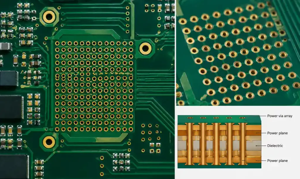
For power delivery vias carrying 1-5 amps, thin annular rings increase via resistance and create hotspots. Use via arrays for redundancy and improved thermal performance.
FAQ
What is the typical registration accuracy for 50-layer PCBs?
Typical registration accuracy is ±100μm (±4 mils) total stack-up tolerance using controlled sequential lamination. This assumes ±50μm per lamination cycle across four build-up stages, calculated using RSS of independent errors.
How do you calculate via capture pad size for high layer count boards?
Use: Drill diameter + 2 × (Min annular ring + Registration tolerance + Drill tolerance + Plating variation). For 50-layer boards with ±100μm registration, a 0.3mm drill requires 0.75-0.80mm capture pads for IPC Class 3 compliance.
What causes registration errors to accumulate?
50-layer PCBs require sequential lamination—building in multiple cycles. Each cycle introduces independent xy-position error from optical alignment limits, thermal expansion during pressing, and resin flow. These combine as RSS, not simple addition.
Can you inspect buried layer registration non-destructively?
3D X-ray laminography can image individual buried layers and measure via-to-pad alignment. However, microsectioning remains the definitive verification method required by IPC-6012.
What IPC standards govern registration tolerances?
IPC-6012 defines registration requirements: Class 1 (±150μm), Class 2 (±75μm), Class 3 (±50μm). IPC-2221 provides capture pad sizing guidelines. IPC-A-600 covers acceptability criteria for measured annular ring.
How does material selection affect registration?
Low-CTE laminates (12-14 ppm/°C) reduce thermal expansion during pressing, cutting thermally-induced error by 25-30%. CTE-matched systems minimize differential expansion between copper-heavy and copper-sparse regions.
Conclusion
50-layer PCB registration accuracy requires understanding tolerance accumulation through sequential lamination, optical alignment capabilities, and thermal effects during pressing. Achievable registration is ±100μm total using controlled processes—not the ±50μm single-layer tolerance many designers assume.
Design viable boards by calculating capture pads based on cumulative tolerance, placing test coupons for verification, and selecting suppliers with proven capability. Registration failures cause expensive rework that proper design rules prevent.
Andwin Circuits offers 50-layer capability with optical registration control and IPC-6012 Class 3 certification. Our sequential lamination process achieves ±50μm per-cycle accuracy for reliable complex multilayer boards.
Contact us today for 50-layer PCB manufacturing with fast 15-day delivery, registration verification, and design-for-manufacturing support.