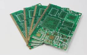
6 layer pcb
1.What is 6-layer pcb
6-layer PCB, or 6-layer printed circuit board, is a multi-layer circuit board widely used in modern electronic devices. It is composed of six layers of conductive materials and insulating materials alternately stacked, usually including four signal layers and two power layers or ground layers. The design and manufacturing process of six-layer PCB is relatively complicated, but its superior performance makes it occupy an important position in high-performance electronic devices.
2.What is the structural composition of a 6-layer PCB?
irst of all, the material selection of 6-layer PCB is crucial. The common substrate is FR-4, which is an epoxy resin material reinforced by glass fiber with good mechanical strength and electrical properties.
In addition, FR-4 material is heat-resistant and chemical-resistant, suitable for most electronic applications. In order to meet the needs of high-frequency applications, high-frequency materials such as PTFE (polytetrafluoroethylene) or ceramic substrates are sometimes used. These materials have lower dielectric constants and dissipation factors, which can effectively reduce losses and interference in signal transmission.
After understanding the materials, let’s explore the structure of 6-layer PCB.
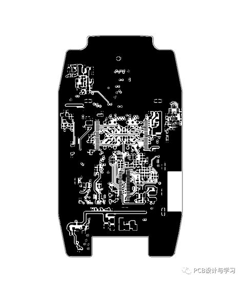
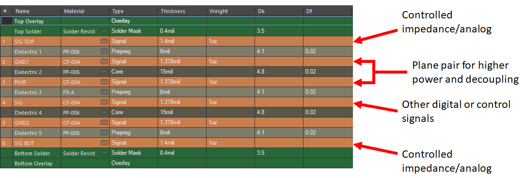
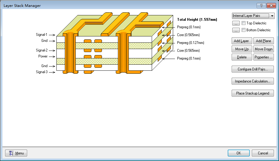
6-layer PCBs are usually composed of six conductive layers and five insulating layers. The outermost layers are the top and bottom layers, which are mainly used to place components and transmit signals.
The middle four layers include two inner signal layers and two power/ground layers. Such a design can not only effectively separate the signal layer and the power layer, reduce electromagnetic interference, but also provide better power distribution and grounding.
GET PCB MANUFACTURING AND ASSEMBLY QUOTE NOW!
3.What are the advantages of 6-layer PCB?
(1)high-density routing capability
(2)achieve more complex circuit designs
(3)reduce signal interference and crosstalk problems, thereby improving the overall performance and reliability of the circuit
4.What are the disadvantages of 6-layer PCB?
(1)increased cost
(2)increased design time and effort required
First of all, a significant advantage of 6-layer PCB is its high-density routing capability. Compared with traditional 2- or 4-layer PCBs, 6-layer PCBs can provide more wiring layers, which allows designers to arrange circuit paths more flexibly to achieve more complex circuit designs.
This high-density wiring capability is particularly suitable for high-performance electronic equipment that requires the integration of a large number of components and complex signal processing, such as computer motherboards, communication equipment and high-end consumer electronics.
However, as wiring density increases, 6-layer PCBs also face some challenges. A major challenge is cost. The materials and processes required to manufacture a 6-layer PCB are more complex than those of a 2-layer or 4-layer PCB, so its production cost is relatively high.
This not only includes the cost of raw materials, but also involves higher manufacturing process requirements and stricter quality control standards. Therefore, for projects with a limited budget, a 6-layer PCB may not be the most economical option.
Nonetheless, the advantages of a 6-layer PCB’s high-density routing capabilities often offset its higher cost. Through more efficient wiring design, 6-layer PCB can significantly reduce signal interference and crosstalk problems, thereby improving the overall performance and reliability of the circuit.
This is particularly important for applications that require high signal integrity, such as high-speed data transmission and radio frequency circuits. In addition, the 6-layer PCB can further improve the electrical performance and thermal management capabilities of the circuit by optimizing the layout of the power supply and ground layers.
When weighing the advantages and disadvantages of a 6-layer PCB, designers need to consider the needs of the specific application and budget constraints.
For example, for those electronic devices that require high performance and reliability, the high-density wiring and superior electrical performance of 6-layer PCB may be indispensable. For projects that are cost-sensitive and have lower circuit complexity, it may be more appropriate to choose a lower-layer PCB.
Overall, 6-layer PCB has significant advantages in terms of high-density wiring and electrical performance, but its higher manufacturing cost also needs to be considered in project planning.
Through reasonable design and optimization, 6-layer PCB can find a balance point between performance and cost to meet the needs of different application scenarios. When designers select the number of PCB layers, they should make the most appropriate decision based on the technical requirements and budget constraints of the specific project.
GET PCB AND ASSEMBLY SERVICE QUOTE NOW!
5.Application of 6-layer PCB
(1)in high-frequency circuit design
(2)also reflected in its optimization of thermal management.
(3)high-frequency circuit design also includes its improvement of electromagnetic compatibility (EMC).
(4)advanced driver-assistance systems
(5) aerospace and defense
In general, the application of 6-layer PCB in high-frequency circuit design has many advantages, including improving signal integrity, optimizing power distribution, improving thermal management and electromagnetic compatibility.
These advantages make 6-layer PCB an indispensable and important component in high-frequency circuit design. By rationally utilizing the multi-layer structure and design methods of 6-layer PCB, designers can better cope with various challenges in high-frequency circuit design, thereby achieving higher performance and more reliable circuit designs.