6-Layer PCB Stackup Design for High-Speed Applications
Introduction
In today’s rapidly advancing electronics industry, high-speed digital designs have become ubiquitous across various applications including networking equipment, telecommunications, computing systems, and advanced consumer electronics. As signal frequencies continue to increase and rise times decrease, proper printed circuit board (PCB) stackup design has emerged as a critical factor in ensuring signal integrity, power integrity, and electromagnetic compatibility (EMC).
The 6-layer PCB stackup has become a popular choice for many high-speed designs, offering an excellent balance between cost, complexity, and performance. This configuration provides sufficient layers for proper signal routing, power distribution, and grounding while remaining more economical than higher layer count boards. When properly designed, a 6-layer stackup can effectively support high-speed signals in the multi-gigahertz range while maintaining signal quality and minimizing electromagnetic interference (EMI).
This article will explore the fundamental considerations, recommended configurations, material selection, and design techniques for implementing an optimal 6-layer PCB stackup for high-speed applications. We will examine various stackup options, analyze their advantages and limitations, and provide practical guidelines for designers working with high-speed signals.
Fundamentals of High-Speed PCB Stackup Design
Signal Integrity Considerations
In high-speed designs, signal integrity (SI) becomes paramount as frequencies increase. Several critical factors must be considered:
- Impedance Control: Maintaining consistent characteristic impedance (typically 50Ω for single-ended and 100Ω for differential pairs) throughout the signal path is essential to prevent reflections. The impedance depends on the trace width, dielectric thickness, and material properties.
- Crosstalk: Unwanted coupling between adjacent signals can cause interference and signal degradation. Proper layer arrangement and spacing can minimize crosstalk.
- Return Path: High-frequency signals follow the path of least inductance, not just least resistance. A continuous return path adjacent to the signal layer is crucial for minimizing loop area and maintaining signal quality.
- Propagation Delay: The time it takes for a signal to travel through a transmission line becomes significant at high speeds and must be matched for differential pairs and timing-critical signals.
Power Integrity Considerations
Proper power distribution is equally important in high-speed designs:
- Low Impedance Power Delivery Network (PDN): The power distribution system must provide stable voltage with minimal impedance across the frequency spectrum of interest.
- Decoupling: Proper placement of decoupling capacitors and power/ground plane capacitance helps maintain power stability.
- Plane Resonance: Power and ground planes can act as resonant cavities at certain frequencies, potentially causing noise amplification.
EMI Considerations
Electromagnetic interference can both affect the board’s operation and cause compliance issues:
- Radiated Emissions: High-speed signals can radiate energy if not properly contained.
- Susceptibility: The board must be protected from external interference.
- Common Mode Noise: Improper return paths can lead to common mode currents that radiate efficiently.
6-Layer Stackup Configurations
Several 6-layer stackup configurations are commonly used in high-speed designs, each with its own advantages and trade-offs. The choice depends on the specific requirements of the design, including signal density, power requirements, and cost constraints.
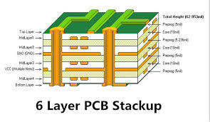
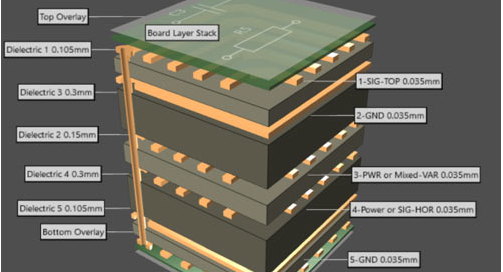
Preferred Configuration: Signal-Power-Ground-Signal-Signal-Ground
Layer 1: Top Signal (Microstrip)
Layer 2: Ground Plane
Layer 3: Power Plane
Layer 4: Signal Layer
Layer 5: Signal Layer
Layer 6: Bottom Signal (Microstrip)
This configuration offers several advantages for high-speed designs:
- Excellent Signal Integrity: The top and bottom layers have adjacent ground planes (Layer 2 for Top, Layer 5 for Bottom) providing solid return paths.
- Controlled Impedance: Both outer layers can be designed as controlled impedance microstrip lines.
- Good Power Distribution: The dedicated power plane in Layer 3 allows for low-impedance power distribution.
- EMI Control: The ground planes help contain electromagnetic fields and reduce radiation.
- Crosstalk Reduction: Sensitive signals can be routed on Layer 1 or 6, with less critical signals on Layers 4 and 5.
The main limitation of this stackup is the lack of stripline routing options, which can be beneficial for very high-speed or noise-sensitive signals. However, for many applications, microstrip routing on the outer layers combined with proper design techniques can provide sufficient performance.
Alternative Configuration: Signal-Ground-Signal-Power-Signal-Ground
Layer 1: Top Signal (Microstrip)
Layer 2: Ground Plane
Layer 3: Signal Layer (Stripline)
Layer 4: Power Plane
Layer 5: Signal Layer (Stripline)
Layer 6: Bottom Signal (Microstrip)
This alternative offers:
- Stripline Routing Options: Layers 3 and 5 are embedded between planes, allowing for stripline routing which offers better EMI performance and less crosstalk than microstrip.
- Good Power Integrity: The power plane is centrally located.
- Flexible Signal Routing: Combination of microstrip and stripline routing options.
The trade-off is slightly more complex manufacturing and potentially higher cost due to the need for more precise layer-to-layer registration.
High-Speed Optimized Configuration
For designs with particularly demanding high-speed requirements, the following stackup can be considered:
Layer 1: Top Signal (Microstrip)
Layer 2: Ground Plane
Layer 3: Signal Layer (Stripline)
Layer 4: Ground Plane
Layer 5: Power Plane
Layer 6: Bottom Signal (Microstrip)
This configuration provides:
- Excellent Signal Integrity: Multiple ground planes provide solid return paths for all signal layers.
- Superior EMI Performance: The additional ground plane helps contain electromagnetic fields.
- Flexible Power Distribution: The power plane can be split for multiple voltages if needed.
The main disadvantage is reduced routing resources compared to other configurations, as one layer is dedicated to an additional ground plane.
Material Selection for High-Speed 6-Layer PCBs
The choice of PCB materials significantly impacts the performance of high-speed designs. Key considerations include:
Dielectric Material Properties
- Dielectric Constant (Dk): Affects signal propagation speed and impedance. Materials with stable Dk across frequency are preferred (e.g., FR-4 with Dk ~4.3 at 1GHz, or high-performance materials with lower Dk).
- Dissipation Factor (Df): Determines dielectric losses. Lower Df is better for high-speed signals (standard FR-4 ~0.02, high-speed versions ~0.01 or lower).
- Thermal Stability: Important for maintaining consistent electrical properties across operating temperatures.
Common Material Options
- Standard FR-4: Cost-effective but with higher loss at multi-GHz frequencies. Suitable for designs up to about 3-5 GHz.
- High-Speed FR-4: Modified versions with improved Dk and Df characteristics. Good balance of performance and cost.
- Rogers, Isola, or other high-performance materials: Offer superior electrical properties but at higher cost. Used for very high-frequency applications (>10 GHz).
Copper Foil Considerations
- Foil Type: Standard electrodeposited (ED) copper or low-profile/ultra-low-profile copper for improved high-frequency skin effect performance.
- Surface Roughness: Smoother copper reduces conductor losses at high frequencies.
- Weight: Typically 1 oz (35 μm) or 0.5 oz (17 μm) for fine features.
Design Guidelines for High-Speed 6-Layer PCBs
Layer Usage and Routing Strategy
- Signal Layers:
- Route critical high-speed signals on outer layers (microstrip) when possible for best signal integrity and easiest access for probing.
- Use inner signal layers (stripline) for less critical signals or when EMI containment is crucial.
- Group signals by speed and sensitivity when assigning layers.
- Ground Planes:
- Keep ground planes intact as much as possible.
- Provide numerous ground vias near signal transitions between layers to maintain return path continuity.
- Avoid splitting ground planes unless absolutely necessary.
- Power Planes:
- Use solid planes for primary power rails.
- Multiple voltages can share a plane if properly partitioned, but avoid creating slots that obstruct return currents.
- Place bypass capacitors strategically to minimize power loop inductance.
Impedance Control
- Calculate and specify controlled impedance requirements for all critical traces during stackup design.
- Account for manufacturing tolerances in dielectric thickness and copper width when calculating target impedances.
- Use field solver tools for accurate impedance calculations, especially for differential pairs or complex geometries.
- Specify impedance requirements clearly in fabrication drawings, including which layers require control and tolerance expectations.
Via Management
- Minimize via transitions for high-speed signals as each via introduces discontinuity.
- Use appropriate via structures:
- Through-hole vias for standard connections
- Blind or buried vias when density requires (increases cost)
- Microvias for very high-density designs
- Provide return vias adjacent to signal vias to maintain return path continuity.
- Consider backdrilling for critical high-speed signals to remove via stubs that can cause reflections.
Power Distribution Network Design
- Implement proper decoupling:
- Use a mix of bulk, ceramic, and high-frequency capacitors
- Place capacitors as close as possible to power pins
- Consider plane capacitance as part of the PDN
- Analyze PDN impedance using simulation tools to ensure target impedance is met across the frequency range of interest.
- Manage plane resonances through proper use of decoupling and possible segmentation damping techniques if needed.
EMI Reduction Techniques
- Implement proper grounding strategies to minimize common-mode currents.
- Use guard traces or ground fences around sensitive or noisy signals when needed.
- Consider edge termination of planes to reduce edge radiation (stitching vias, absorbing materials).
- Route sensitive signals on stripline layers when EMI is a particular concern.
Manufacturing Considerations
Tolerances and Stackup Symmetry
- Maintain symmetry in the layer stackup to prevent warpage during manufacturing and assembly.
- Account for manufacturing tolerances in dielectric thickness (±10% is typical).
- Specify copper weights clearly for each layer.
- Consider final finish options (ENIG, Immersion Silver, OSP, etc.) and their impact on signal integrity.
Documentation Requirements
- Provide detailed stackup drawing including:
- Layer materials and thicknesses
- Copper weights
- Impedance requirements
- Special material requirements
- Clearly identify critical signals and their requirements.
- Specify any special manufacturing processes (backdrilling, via filling, etc.).
Simulation and Verification
Pre-layout Simulation
- Perform stackup simulations to verify impedance targets and coupling characteristics.
- Model transmission line structures to ensure proper performance.
- Simulate power distribution network to verify low impedance across target frequency range.
Post-layout Verification
- Perform signal integrity analysis on critical nets to verify performance.
- Check for timing violations on high-speed parallel buses.
- Verify power integrity through simulation of the complete PDN.
- Conduct EMI analysis if required by the application.
Conclusion
Designing an effective 6-layer PCB stackup for high-speed applications requires careful consideration of signal integrity, power integrity, and EMI requirements. The preferred stackup configuration with signal layers adjacent to continuous ground planes provides an excellent balance of performance and manufacturability for most high-speed designs.
By following the guidelines presented in this article—selecting appropriate materials, implementing proper layer usage strategies, controlling impedances, managing vias, and designing a robust power distribution network—designers can create 6-layer PCBs that successfully meet the challenges of modern high-speed digital systems.
Remember that each design has unique requirements, and the optimal stackup may vary depending on specific application needs. Simulation and prototyping remain essential tools for verifying performance before committing to production. As signal speeds continue to increase, the principles of good stackup design will remain fundamental to successful high-speed PCB implementation.