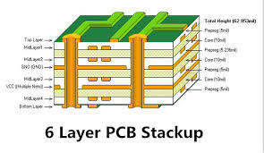
6 layer pcb stackup for high speed
Key points of 6 layer PCB stacking design in high-frequency and high-speed circuits. In the design of high-frequency and high-speed circuits, the selection of 6-layer PCB stacking structure is crucial,6 layer pcb stackup for high speed。

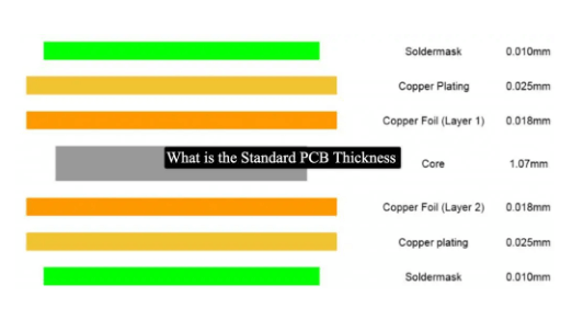
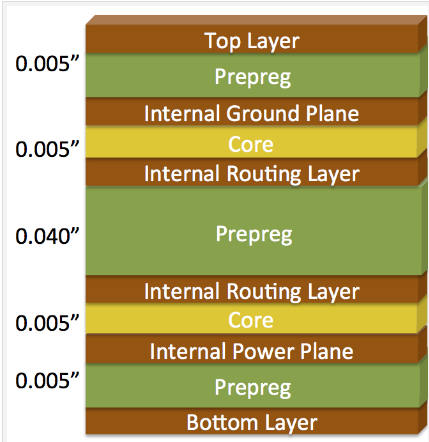
.First of all, a reasonable stacking design can effectively reduce signal interference and electromagnetic radiation, thereby improving the overall performance of the circuit. Usually, the 6-layer PCB stacking structure includes two signal layers, two power layers, and two ground layers. With this configuration, the optimization of signal integrity and power integrity can be achieved.
Next, the layout of the signal layer is a key link in the design. In order to reduce crosstalk between signals, the signal layer should be kept as far away from the power layer and the ground layer as possible. Usually, the signal layer is placed on the outermost layer, while the power layer and the ground layer are placed in the middle layer. In this way, the distance between the signal layers is increased, reducing the coupling effect between the signals. In addition, the routing of the signal layer should be as short and straight as possible to reduce the delay and loss of signal transmission.
、
At the same time, the design of the power layer and the ground layer should not be ignored.
The power layer and the ground layer should be as close as possible to form a low-impedance power loop. This not only helps to reduce power supply noise, but also improves the stability of the power supply. Usually, the distance between the power layer and the ground layer should be as small as possible to form a tightly coupled structure. In addition, the copper foil thickness of the power layer and the ground layer should be appropriate to ensure sufficient current carrying capacity.
In high-frequency and high-speed circuits, signal integrity is an important consideration.
In order to ensure the integrity of the signal, signal reflection and crosstalk should be avoided as much as possible in the design. Through reasonable stacking design, signal reflection and crosstalk can be effectively reduced. For example, adding a dielectric layer between the signal layer and the ground layer can effectively reduce signal reflection. In addition, the routing of the signal layer should try to avoid sharp turns to reduce signal reflection and loss.
In addition, electromagnetic compatibility (EMC) is also an important aspect in high-frequency and high-speed circuit design.
Through reasonable stacking design, electromagnetic radiation and interference can be effectively reduced. For example, adding a shielding layer between the signal layer and the ground layer can effectively reduce electromagnetic radiation. In addition, the design of the power layer and the ground layer should be as close as possible to form a low-impedance power loop, thereby reducing electromagnetic interference.
In short, in high-frequency and high-speed circuit design, the selection and design of the 6-layer PCB stacking structure is crucial.
Through reasonable stacking design, signal integrity and power integrity can be effectively improved, signal interference and electromagnetic radiation can be reduced, and the overall performance of the circuit can be improved. By paying attention to the proper arrangement of signal layers, power layers, and ground layers, the optimized design of high-frequency and high-speed circuits can be achieved.
In high-frequency applications, the key points of 6-layer PCB stacking design are crucial because it directly affects signal integrity, electromagnetic compatibility, and overall circuit performance.
First, a reasonable stacking structure is the basis for ensuring signal integrity. Generally, the stacking structure of a 6-layer PCB includes two signal layers, two power layers, and two ground layers. With this configuration, interference between signals can be effectively reduced, and a stable power and ground reference can be provided.
Second, the layout of the signal layer requires special attention. In high-frequency applications, the path of signal transmission should be as short and straight as possible to reduce signal reflection and loss. To achieve this goal, designers should place high-speed signals on the inner layer to provide shielding using the ground plane on the outer layer. In addition, the spacing between signal layers should be as small as possible to reduce signal crosstalk.
The 6-layer PCB stacking design in high-frequency applications requires comprehensive consideration of multiple factors such as signal integrity, power stability, and electromagnetic compatibility.
Excellent performance of high-frequency circuits can be ensured through reasonable stacking structure, fine signal layout, tight power and ground coupling, careful use of vias, and effective simulation and testing.