6 Major Factors of Post-check of PCB Design
In the PCB design process, once a PCB board has completed layout and routing, and the connectivity and spacing have been checked without error, is the PCB completed? The answer is of course no. Many beginners, including some experienced engineers, often rush through the process and ignore post-check due to time constraints, impatience or overconfidence. As a result, some very basic bugs appear, such as insufficient line width, component number silk screen pressed on vias, sockets too close together, signal loops, etc. This leads to electrical problems or process problems, and serious problems require re-boarding, resulting in waste. Therefore, after a PCB has completed layout and routing, a very important step is post-check.
There are many detailed factors in PCB design inspection. This article lists some of the most basic and most error-prone factors as post-check.
1.Component package
(1) Pad spacing. If it is a new device, you need to draw the component package yourself to ensure that the spacing is appropriate. The pad spacing directly affects the soldering of the component.
(2) Via size (if any). For plug-in devices, the size of the via should have enough margin, and it is generally appropriate to keep no less than 0.2mm.
(3) Outline silk screen. The outline silk screen of the device should be slightly larger than the actual size to ensure that the device can be installed smoothly.
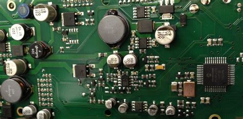
2.PCB layout
(1) IC should not be close to the edge of the board.
(2) Devices of the same module circuit should be placed close to each other. For example, the decoupling capacitor should be close to the power pin of the IC. Devices that make up the same functional circuit should be placed in the same area with clear layers to ensure the realization of the function.
(3) Arrange the position of the socket according to the actual installation. The sockets are all wired to other modules. According to the actual structure, in order to facilitate installation, the position of the socket is generally arranged according to the principle of proximity, and it is generally close to the edge of the board.
(4) Pay attention to the direction of the socket. The socket has a direction. If the direction is reversed, the wire material must be re-customized. For flat-plug sockets, the socket direction should face the outside of the board.
(5) There should be no devices in the Keep Out area.
(6) The interference source should be away from sensitive circuits. High-speed signals, high-speed clocks, or high-current switching signals are all interference sources and should be kept away from sensitive circuits, such as reset circuits and analog circuits. Grounding can be used to separate them.
3.PCB wiring
(1) Line width. The line width should be selected in combination with the process and current carrying capacity. The minimum line width cannot be less than the minimum line width of the PCB manufacturer. At the same time, the current carrying capacity should be guaranteed. Generally, 1mm/A is used to select the appropriate line width.
(2) Differential signal lines. For differential lines such as USB and Ethernet, pay attention to the equal length, parallel, and coplanar routing. The spacing is determined by the impedance.
(3) Pay attention to the return path for high-speed lines. High-speed lines are prone to electromagnetic radiation. If the area formed by the routing path and the return path is too large, a single-turn coil will be formed to radiate electromagnetic interference outward, as shown in Figure 1. Therefore, when routing, pay attention to the return path next to it. The multilayer board with power layer and ground plane can effectively solve this problem.
(4) Pay attention to analog signal lines. Analog signal lines should be separated from digital signals. Avoid routing lines near interference sources (such as clocks and DC-DC power supplies) as much as possible, and the shorter the lines, the better.
4.EMC and signal integrity
(1) Termination resistor. For high-speed lines or digital signal lines with high frequencies and long routing, it is best to insert a matching resistor in series at the end.
(2) Connect a small capacitor to the input signal line. For the signal line input from the interface, it is best to connect a small capacitor of the picofarad level near the interface. The size of the capacitor depends on the strength and frequency of the signal and cannot be too large, otherwise it will affect the signal integrity. For low-speed input signals, such as key input, a small capacitor of 330pF can be used, as shown in Figure 2.
(3) Driving capability. For example, a switch signal with a large driving current can be driven by a transistor; for a bus with a large fan-out number, a buffer (such as 74LS224) can be added to drive it.

5.Silkscreen
(1) Board name, time, PN code.
(2) Labeling. Label the pins or key signals of some interfaces (such as arrays).
(3) Component numbers. Component numbers should be placed in appropriate locations. Dense component numbers can be placed in groups. Be careful not to place them at the via position.
6.Others
Mark points. For PCBs that require machine soldering, two or three mark points need to be added.