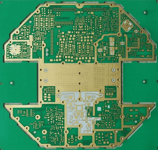
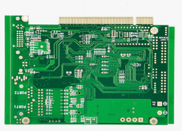
7 series pcb design guide
7 Series PCB Design Guide: Tips and Techniques for Optimizing Signal Integrity
When designing 7 series PCBs, optimizing signal integrity is an important step to ensure the performance and reliability of the board.
- First, such as FR4, choosing the right material is crucial for signal integrity.
High-frequency signal transmission requires low-loss dielectric materials to reduce signal attenuation and distortion. Although common materials are low-cost, they may not be ideal in high-frequency applications, so higher-performance materials such as Rogers or ceramic substrates can be considered.
- Next, the routing strategy is one of the key factors affecting signal integrity.
To reduce signal reflection and crosstalk, designers should try to keep the length of signal lines consistent and avoid sharp corners. Using differential pair routing can effectively reduce electromagnetic interference (EMI) and improve the signal’s anti-interference ability. In addition, keeping the signal line closely coupled to the ground line helps reduce impedance mismatch, thereby reducing signal reflection.
- Transitioning to the design of the power and ground planes, it is equally important to ensure the integrity of the power and ground planes.
Splitting the power and ground planes will lead to an increase in power supply noise and ground bounce noise, which will affect signal integrity. Therefore, designers should try to avoid splitting the power and ground planes, and ensure that there are sufficient decoupling capacitors between the power and ground planes to smooth out the power supply noise.
- In addition, the use of vias also needs to be cautious.
Vias introduce parasitic inductance and capacitance, affecting the transmission of high-frequency signals. To reduce these effects, blind and buried via technologies can be used to reduce the number of vias in the signal path. At the same time, try to avoid using vias on high-speed signal paths, or use multiple vias in parallel when necessary to reduce parasitic effects.
- In signal integrity analysis, the use of simulation tools is indispensable.
Through simulation tools, designers can predict and analyze signal integrity problems in the design stage, so as to optimize and adjust before actual manufacturing. This not only saves time and cost, but also improves the reliability and performance of the design.
- Finally, testing and verification are the final steps to ensure signal integrity.
Signal integrity testing on the actual manufactured PCB can verify the effectiveness of the design. Using test equipment such as oscilloscopes and network analyzers, the time domain and frequency domain characteristics of the signal can be detected to ensure the quality of signal transmission.
In summary, optimizing signal integrity in 7 series PCB design requires comprehensive consideration of material selection, routing strategy, power and ground plane design, via usage, simulation analysis, and test verification. Through systematic methods and techniques, designers can effectively improve the performance and reliability of PCBs to meet the needs of high-frequency applications.
In 7 series PCB design, power management is a crucial link, which directly affects the performance and reliability of the circuit board.
- Reasonable power distribution is the basis of power management.
In order to ensure that each component can operate stably, the designer needs to reasonably distribute the power according to the voltage and current requirements of different components. By using a multi-layer PCB, the power and ground lines can be effectively separated to reduce power noise and ground interference
- The selection and layout of power decoupling capacitors are also key steps in power management.
Decoupling capacitors can filter out high-frequency noise in the power supply and stabilize the voltage. Usually, designers will place decoupling capacitors near the power pins of each IC to ensure the stability of the power supply. Choose the appropriate capacitance value and type, such as ceramic capacitors and tantalum capacitors, which can be adjusted according to specific circuit requirements. In addition, the layout of the decoupling capacitors also needs to be paid attention to, as close as possible to the power pins of the IC to reduce the influence of parasitic inductance.
- The design of the power plane is also an important link in power management.
The power plane can provide a low-impedance power path and reduce power noise. Designers need to ensure that the distance between the power plane and the ground plane is as small as possible to reduce the parasitic inductance between the power supply and the ground. At the same time, the power plane needs to be as complete as possible to avoid unnecessary cutting and segmentation to ensure the continuity and stability of the power supply.
In power management, power filtering is also an important part that cannot be ignored. The power filter can effectively filter out low-frequency and high-frequency noise in the power supply and provide clean power. Common power filters include LC filters and RC filters. Designers can choose the appropriate filter type and parameters according to specific circuit requirements. In addition, the layout of the filter also needs to be paid attention to, and it should be as close to the power input as possible to improve the filtering effect.


