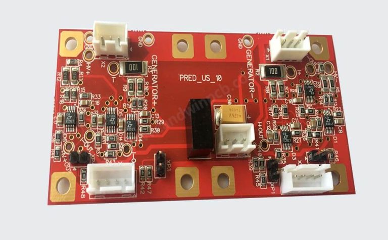
7 steps to teach you how to design a perfect PCB
PCB has developed from single-layer to double-sided, multi-layer and flexible, and still maintains its own development trend. Due to the continuous development towards high precision, high density and high reliability, the continuous reduction of size, reduction of cost and improvement of performance, the printed circuit board still maintains a strong vitality in the development of future electronic equipment.
So how is PCB designed? You will understand after reading the following seven steps:
- Preliminary preparation
Includes preparation of component library and schematic diagram. Before PCB design, first prepare the schematic diagram SCH component library and PCB component package library.
It is best for engineers to establish the PCB component package library based on the standard size data of the selected device. In principle, first establish the PC component package library, and then establish the schematic diagram SCH component library.
The PCB component package library has high requirements, which directly affects the installation of the PCB; the schematic diagram SCH component library has relatively loose requirements, but it is important to define the pin attributes and the corresponding relationship with the PCB component package library.
- PCB structure design
According to the determined circuit board size and various mechanical positioning, draw the PCB board frame in the PCB design environment, and place the required connectors, buttons/switches, screw holes, assembly holes, etc. according to the positioning requirements.
Fully consider and determine the wiring area and non-wiring area (such as how much area around the screw hole belongs to the non-wiring area).
- PCB layout design
Layout design is to place components in the PCB board frame according to design requirements. Generate a network table in the schematic tool (Design→Create Netlist), and then import the network table in the PCB software (Design→Import Netlist). After the network table is successfully imported, it will exist in the software background. Through the Placement operation, all devices can be called out, and there will be flying wire prompts between each pin. At this time, the device layout design can be performed.
PCB layout design is the first important process in the entire PCB design process. The more complex the PCB board, the more directly the layout will affect the difficulty of later wiring.
Layout design relies on the circuit foundation and design experience of the circuit board designer, and it is a higher level requirement for the circuit board designer. Junior circuit board designers have little experience and are suitable for small module layout design or PCB layout design tasks with low difficulty for the whole board.
- PCB wiring design
PCB wiring design is the most labor-intensive process in the entire PCB design, which directly affects the performance of the PCB board.
In the design process of PCB, there are generally three levels of wiring:
First, wiring is smooth, which is the most basic entry requirement for PCB design;
Second, electrical performance is satisfied, which is the standard for measuring whether a PCB board is qualified. After the line is smooth, the wiring is carefully adjusted to achieve the best electrical performance;
Third, it is neat and beautiful. Even if the electrical performance is good, the messy wiring will bring great inconvenience to the later board optimization, testing and maintenance. The wiring requirements are uniform and cannot be crisscrossed without any rules.
- Wiring optimization and silk screen placement
“PCB design has no best, only better”, “PCB design is an art of defects”, which is mainly because PCB design needs to realize the design requirements of all aspects of hardware, and individual requirements may conflict with each other, and you can’t have your cake and eat it too.
For example: a PCB design project needs to be designed as a 6-layer board after evaluation by the circuit board designer, but the product hardware must be designed as a 4-layer board for cost considerations, so the signal shielding ground layer can only be sacrificed, which will increase the signal crosstalk between adjacent wiring layers and reduce the signal quality.
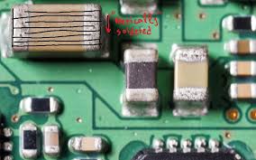
The general design experience is: the time for optimizing wiring is twice the time for initial wiring. After the PCB wiring optimization is completed, post-processing is required. The first thing to deal with is the silk screen logo on the PCB board. When designing, the silk screen characters on the bottom layer need to be mirrored to avoid confusion with the top layer silk screen.
- Network DRC inspection and structural inspection
Quality control is an important part of the PCB design process. General quality control methods include: design self-inspection, design mutual inspection, expert review meeting, special inspection, etc.
Schematic diagram and structural element diagram are the most basic design requirements. Network DRC inspection and structural inspection are to confirm that the PCB design meets the two input conditions of schematic netlist and structural element diagram respectively.
Generally, circuit board designers will have their own accumulated design quality inspection checklist, some of which are derived from the company or department’s specifications, and the other part is derived from their own experience summary. Special inspections include Valor inspection and DFM inspection of the design. These two parts focus on the back-end processing photolithography files of PCB design output.
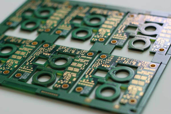
- PCB board making
Before the formal processing of PCB board making, the circuit board designer needs to communicate with the PE of the PCB A board factory and answer the manufacturer’s confirmation questions about PCB board processing.
These include but are not limited to: selection of PCB board model, adjustment of line width and line spacing of circuit layers, adjustment of impedance control, adjustment of PCB stacking thickness, surface treatment processing technology, aperture tolerance control and delivery standards, etc.