8 Layer PCB Fabrication: A Comprehensive Guide
Printed Circuit Boards (PCBs) are the backbone of modern electronics, providing the necessary platform for electrical connections and mechanical support for electronic components. As technology advances, the complexity of electronic devices increases, leading to the need for more sophisticated PCBs. One such advanced PCB is the 8-layer PCB, which offers enhanced functionality, improved signal integrity, and greater design flexibility compared to its single or double-layer counterparts. This article delves into the intricacies of 8-layer PCB fabrication, covering the design considerations, materials, manufacturing processes, and quality control measures involved in producing these complex boards.
1. Introduction to 8-Layer PCBs
An 8-layer PCB is a multilayer board consisting of eight conductive layers separated by insulating materials. These layers are interconnected through vias, which are small holes filled with conductive material to allow electrical connections between layers. The additional layers in an 8-layer PCB provide more routing options, reduce electromagnetic interference (EMI), and improve the overall performance of the circuit.
2. Design Considerations for 8-Layer PCBs
Designing an 8-layer PCB requires careful planning and consideration of various factors to ensure optimal performance and manufacturability. Key design considerations include:
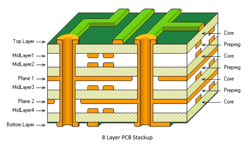
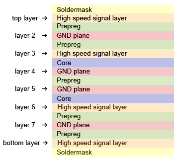
2.1 Layer Stackup
The layer stackup defines the arrangement of the conductive and insulating layers in the PCB. A typical 8-layer stackup might include the following layers:
- Top Layer (Signal Layer): This layer is used for placing components and routing high-speed signals.
- Ground Plane (GND): Provides a reference plane for signal return paths and reduces EMI.
- Inner Signal Layer 1: Used for routing signals.
- Power Plane (VCC): Distributes power to the components.
- Inner Signal Layer 2: Another layer for routing signals.
- Ground Plane (GND): Another ground plane for additional shielding.
- Inner Signal Layer 3: Used for routing signals.
- Bottom Layer (Signal Layer): Similar to the top layer, used for placing components and routing signals.
The specific stackup may vary depending on the design requirements, such as the need for impedance control, signal integrity, and thermal management.
2.2 Signal Integrity
Signal integrity is critical in high-speed designs. To maintain signal integrity, designers must consider:
- Impedance Control: Matching the impedance of transmission lines to the source and load impedances to minimize reflections.
- Crosstalk: Reducing crosstalk by maintaining adequate spacing between signal traces and using ground planes as shields.
- Signal Routing: Routing high-speed signals on inner layers between ground and power planes to reduce EMI.
2.3 Power Integrity
Power integrity ensures that the power distribution network (PDN) delivers stable and clean power to all components. Key considerations include:
- Decoupling Capacitors: Placing decoupling capacitors close to power pins to reduce noise.
- Power Plane Design: Ensuring low impedance paths for power distribution by using wide traces or planes.
- Voltage Drop: Minimizing voltage drop by using appropriate trace widths and copper weights.
2.4 Thermal Management
Thermal management is crucial to prevent overheating and ensure reliable operation. Designers should consider:
- Thermal Vias: Using thermal vias to transfer heat from components to inner or bottom layers.
- Copper Pour: Adding copper pour on unused areas of the PCB to dissipate heat.
- Component Placement: Placing heat-generating components away from sensitive areas and ensuring adequate airflow.
3. Materials Used in 8-Layer PCB Fabrication
The choice of materials significantly impacts the performance and reliability of an 8-layer PCB. Common materials include:
3.1 Substrate Material
The substrate, or base material, is typically made of FR-4, a flame-retardant epoxy laminate reinforced with glass fiber. FR-4 offers a good balance of electrical insulation, mechanical strength, and thermal stability. For high-frequency applications, materials with lower dielectric constants, such as Rogers or Teflon, may be used.
3.2 Copper Foil
Copper foil is used for the conductive layers. The thickness of the copper foil is specified in ounces per square foot (oz/ft²), with common thicknesses being 0.5 oz, 1 oz, and 2 oz. Thicker copper foils are used for higher current-carrying capacity.
3.3 Prepreg and Core
Prepreg (pre-impregnated) and core materials are used to bond the layers together. Prepreg is a fiberglass material impregnated with resin, while the core is a fully cured laminate with copper foil on both sides. The choice of prepreg and core materials affects the dielectric constant, thermal properties, and mechanical stability of the PCB.
3.4 Solder Mask
The solder mask is a protective layer applied over the copper traces to prevent solder bridging and protect against environmental factors. Common solder mask colors include green, blue, red, and black.
3.5 Silkscreen
The silkscreen layer is used for printing component designators, logos, and other markings on the PCB. It is typically applied using epoxy ink.
4. Manufacturing Process of 8-Layer PCBs
The fabrication of an 8-layer PCB involves several complex steps, each requiring precision and attention to detail. The key steps in the manufacturing process are:
4.1 Design and Layout
The process begins with the design and layout of the PCB using Computer-Aided Design (CAD) software. The design includes the placement of components, routing of traces, and definition of vias. Design for Manufacturability (DFM) checks are performed to ensure the design can be reliably manufactured.
4.2 Layer Preparation
Each layer of the PCB is prepared separately. The copper foil is laminated onto the substrate, and the desired circuit pattern is transferred onto the copper using photolithography. The unwanted copper is etched away, leaving only the desired traces.
4.3 Layer Alignment and Lamination
The individual layers are aligned using registration holes and laminated together under heat and pressure. The prepreg material bonds the layers together, forming a solid multilayer structure.
4.4 Drilling
Holes are drilled through the laminated board to create vias and through-holes for component leads. The drilling process must be precise to ensure proper alignment and connectivity between layers.
4.5 Plating
The drilled holes are plated with copper to create electrical connections between layers. This process involves electroless copper deposition followed by electroplating to build up the copper thickness.
4.6 Outer Layer Imaging and Etching
The outer layers are coated with a photoresist, and the circuit pattern is transferred using photolithography. The unwanted copper is etched away, leaving the final circuit pattern on the outer layers.
4.7 Solder Mask Application
The solder mask is applied over the outer layers, leaving only the pads and vias exposed. The solder mask is cured using UV light.
4.8 Surface Finish
A surface finish is applied to the exposed copper pads to protect them from oxidation and improve solderability. Common surface finishes include HASL (Hot Air Solder Leveling), ENIG (Electroless Nickel Immersion Gold), and OSP (Organic Solderability Preservative).
4.9 Silkscreen Printing
The silkscreen layer is printed onto the PCB to add component designators, logos, and other markings.
4.10 Electrical Testing
The finished PCB undergoes electrical testing to verify connectivity and functionality. Automated Optical Inspection (AOI) and Electrical Testing (ET) are commonly used to detect defects and ensure quality.
4.11 Final Inspection and Packaging
The PCB is inspected for any visual defects, such as scratches or misalignments. Once approved, the PCB is packaged and shipped to the customer.
5. Quality Control in 8-Layer PCB Fabrication
Quality control is critical in the fabrication of 8-layer PCBs to ensure reliability and performance. Key quality control measures include:
5.1 Design Review
A thorough design review is conducted to identify potential issues before fabrication begins. This includes checking for proper layer stackup, impedance control, and thermal management.
5.2 In-Process Inspection
In-process inspections are performed at various stages of fabrication to detect and correct defects early. This includes checking layer alignment, drilling accuracy, and plating quality.
5.3 Electrical Testing
Electrical testing verifies the connectivity and functionality of the PCB. This includes continuity testing, impedance testing, and high-voltage testing.
5.4 Final Inspection
A final visual inspection is conducted to ensure the PCB meets all specifications and quality standards. This includes checking for proper solder mask application, surface finish, and silkscreen printing.
6. Challenges in 8-Layer PCB Fabrication
Fabricating 8-layer PCBs presents several challenges, including:
6.1 Layer Alignment
Accurate alignment of the layers is crucial to ensure proper connectivity and signal integrity. Misalignment can lead to open circuits or short circuits.
6.2 Thermal Management
Managing heat dissipation in an 8-layer PCB is more complex due to the increased number of layers and components. Proper thermal vias and copper pour are essential to prevent overheating.
6.3 Signal Integrity
Maintaining signal integrity in high-speed designs requires careful routing, impedance control, and crosstalk mitigation. Any deviations can lead to signal degradation and performance issues.
6.4 Manufacturing Complexity
The increased number of layers and the complexity of the design make the manufacturing process more challenging. Precision and attention to detail are required at every step to ensure a high-quality product.
7. Applications of 8-Layer PCBs
8-layer PCBs are used in a wide range of applications, including:
7.1 Telecommunications
Telecommunication equipment, such as routers, switches, and base stations, often require 8-layer PCBs to handle high-speed signals and complex routing.
7.2 Aerospace and Defense
Aerospace and defense applications demand high reliability and performance, making 8-layer PCBs ideal for avionics, radar systems, and communication equipment.
7.3 Medical Devices
Medical devices, such as imaging systems and patient monitoring equipment, require high-density and high-performance PCBs, which 8-layer PCBs can provide.
7.4 Consumer Electronics
High-end consumer electronics, such as smartphones, tablets, and gaming consoles, often use 8-layer PCBs to accommodate the increasing complexity and functionality of these devices.
7.5 Automotive
Modern vehicles, with their advanced electronics and communication systems, rely on 8-layer PCBs for engine control units, infotainment systems, and advanced driver-assistance systems (ADAS).
8. Conclusion
The fabrication of 8-layer PCBs is a complex and intricate process that requires careful design, precise manufacturing, and rigorous quality control. These advanced PCBs offer numerous benefits, including improved signal integrity, enhanced functionality, and greater design flexibility, making them essential for a wide range of high-performance applications. As technology continues to evolve, the demand for 8-layer PCBs is expected to grow, driving further advancements in PCB fabrication techniques and materials. By understanding the key considerations and challenges involved in 8-layer PCB fabrication, designers and manufacturers can produce high-quality, reliable PCBs that meet the ever-increasing demands of modern electronics.


