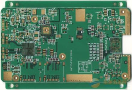
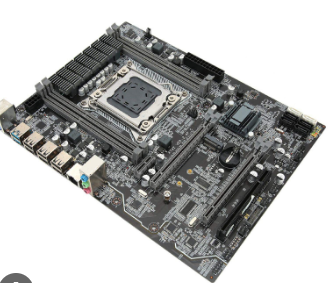
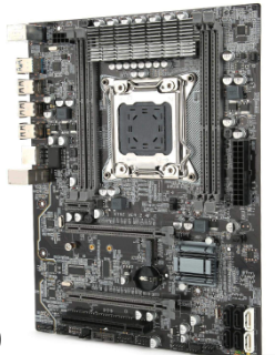
8 layer pcb motherboard
The design and manufacturing process of the 8-layer PCB motherboard is a complex and sophisticated process involving multiple steps and technologies.
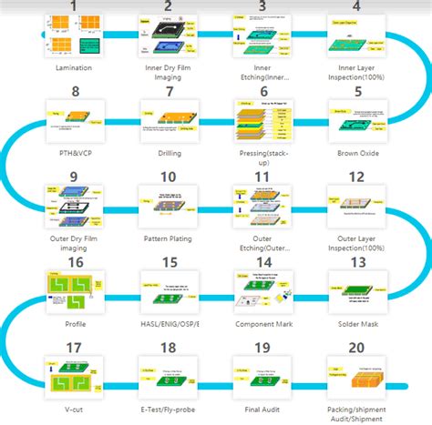
First of all, the design stage is the basis of the entire manufacturing process.
Designers need to use professional electronic design automation (EDA) software to create circuit diagrams and layouts. This stage not only needs to consider the function of the circuit, but also ensure signal integrity and electromagnetic compatibility. Through reasonable stacking structure design, signal interference and crosstalk can be effectively reduced, thereby improving the performance and reliability of the circuit.
Next, the selection of materials is a crucial link.
The 8-layer PCB motherboard usually uses FR4 material, which has good electrical properties and mechanical strength. In addition, it is necessary to select a suitable copper foil thickness to meet the current carrying capacity and heat dissipation requirements. The choice of materials directly affects the performance and cost of the PCB, so it is necessary to find a balance between performance and economy.
After the design and material selection are completed, the manufacturing stage is entered.
The first is the production of the inner layer. The inner layer production includes steps such as pattern transfer, etching and lamination. Graphic transfer is to transfer the designed circuit diagram to the copper foil through photolithography technology, and then remove the excess copper through the etching process to form a circuit pattern. Next, multiple inner layers are stacked together through a lamination process to form a multi-layer structure.
After lamination, drilling and electroplating are performed.
Drilling is to establish electrical connections between different layers, and a high-precision CNC drilling machine is usually used. After drilling, electroplating is required to form a conductive layer on the hole wall to achieve interlayer connection. The electroplating process needs to be strictly controlled to ensure the uniformity and conductivity of the hole wall.
Subsequently, the outer layer is made and surface treated.
The outer layer is made similar to the inner layer, including pattern transfer and etching. Surface treatment is to protect the copper surface. Common methods include hot air leveling (HASL) and electroless nickel gold (ENIG). Different surface treatment methods have different advantages and disadvantages, and the appropriate method needs to be selected according to the specific application.
Finally, testing and quality control are performed.
Testing includes electrical testing and functional testing to ensure that the electrical performance and function of the PCB meet the design requirements. Quality control runs through the entire manufacturing process, from material inspection to finished product inspection, and every link needs to be strictly controlled to ensure the quality of the final product.
In summary, the design and manufacturing process of 8-layer PCB motherboard is a multi-step, precise and complex process. Each link requires a high degree of expertise and technical support, from design, material selection to manufacturing and quality control, each step is crucial. Through scientific and reasonable design and strict manufacturing process, high-performance and high-reliability 8-layer PCB motherboards can be produced to meet the needs of various complex electronic devices.