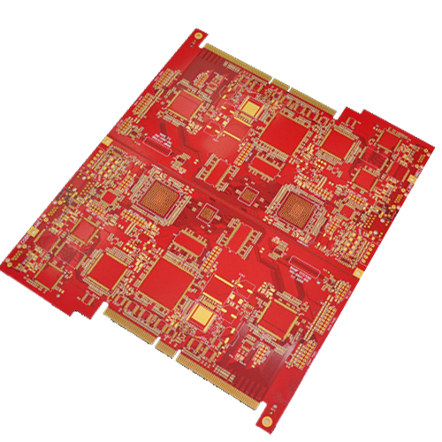
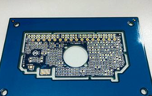
8 layer pcb prototype
It is crucial to understand the key steps and precautions when designing an 8 layer PCB prototype.
First, the designer needs to clarify the functional and performance requirements of the circuit board. This includes determining the basic parameters such as the size, number of layers, materials, and electrical performance of the circuit board. Through a detailed demand analysis, the designer can lay a solid foundation for subsequent design work.
Next, the designer should draw the circuit schematic. This step requires the designer to present all electronic components and their connection relationships in a graphical manner. The accuracy of the schematic directly affects the correctness of the subsequent PCB layout, so every connection point and component parameters must be carefully checked during the drawing process.
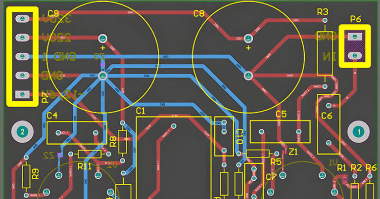
After completing the schematic, the designer needs to design the PCB layout. The layout design should not only consider the reasonable placement of components, but also ensure the shortest and optimal signal path. Especially in the 8-layer PCB design, the interference and electromagnetic compatibility of inter-layer signals are particularly important. Therefore, the designer should reasonably allocate the functions of each layer, such as placing the power layer and the ground layer in the middle layer to reduce signal interference.
Subsequently, the designer needs to design the wiring. Wiring design is the most critical step in PCB design, which directly affects the performance and reliability of the circuit board. In 8-layer PCB, wiring design needs to pay special attention to signal integrity and impedance matching. By using differential signal pairs and controlling line width and line spacing, designers can effectively reduce signal reflection and crosstalk.
After completing the wiring design, designers should perform electrical rule checking (ERC) and design rule checking (DRC). These two inspection steps can help designers find and correct potential problems in the design and ensure that the design of the circuit board meets the manufacturing process and electrical performance requirements. Through strict inspection, designers can greatly improve the success rate and reliability of the circuit board.
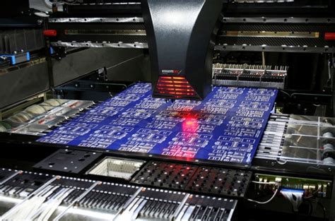
Finally, designers need to generate production files and make samples. Production files include Gerber files, drilling files, and assembly files, etc., which will be directly used for the manufacture and assembly of circuit boards. During the sample production process, designers should pay close attention to the feedback from manufacturers and adjust the design in time to solve possible problems.
In summary, 8-layer PCB prototype design is a complex and delicate process, and each step requires the designer’s meticulousness and expertise. By strictly following the design process and paying attention to key details, designers can ensure that the final circuit board has excellent performance and reliability.