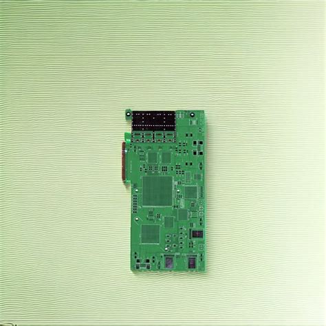
8 layer pcb prototype
Advantages Of Using An 8-Layer PCB Prototype In Complex Circuit Designs
In the realm of modern electronics, the demand for more compact, efficient, and powerful devices has led to the evolution of printed circuit boards (PCBs) from simple single-layer designs to complex multi-layer configurations. Among these, the 8-layer PCB prototype stands out as a particularly advantageous option for complex circuit designs. This configuration offers a multitude of benefits that cater to the intricate needs of advanced electronic applications.
To begin with, one of the primary advantages of using an 8-layer PCB prototype is its ability to support high-density interconnections.
As electronic devices become more sophisticated, the need for increased component density on PCBs becomes paramount. An 8-layer PCB provides ample space for routing complex circuits, allowing designers to incorporate more components without compromising on performance. This is particularly beneficial in applications such as telecommunications, aerospace, and medical devices, where space constraints are a significant concern.
Moreover, the enhanced signal integrity offered by an 8-layer PCB is another compelling reason for its adoption in complex circuit designs.
With multiple layers available, designers can allocate specific layers for power and ground planes, which helps in reducing electromagnetic interference (EMI) and crosstalk between signals. This results in cleaner signal transmission and improved overall performance of the electronic device. Additionally, the ability to separate signal layers with dedicated ground planes aids in maintaining signal integrity, which is crucial for high-speed applications.
Transitioning to another advantage, thermal management is a critical aspect of PCB design, especially in high-power applications.
An 8-layer PCB prototype excels in this regard by providing better heat dissipation capabilities. The additional layers allow for the incorporation of thermal vias and heat sinks, which facilitate efficient heat distribution across the board. This not only enhances the reliability of the device but also extends its operational lifespan by preventing overheating issues.
Furthermore, the flexibility in design that an 8-layer PCB offers cannot be overstated.
With more layers at their disposal, designers have the freedom to implement complex routing strategies and optimize the layout for specific applications. This flexibility is particularly advantageous in prototyping stages, where design iterations are frequent, and modifications are often necessary to achieve the desired performance. The ability to experiment with different configurations without significant constraints is a valuable asset in the development of cutting-edge technologies.
In addition to these technical benefits, the use of an 8-layer PCB prototype can also lead to cost savings in the long run.
While the initial manufacturing cost may be higher compared to simpler PCB designs, the improved performance, reliability, and reduced need for additional components can offset these costs. By integrating more functionality into a single board, designers can minimize the need for external connections and components, ultimately leading to a more streamlined and cost-effective solution.
In conclusion, the advantages of using an 8-layer PCB prototype in complex circuit designs are manifold. From supporting high-density interconnections and enhancing signal integrity to improving thermal management and offering design flexibility, this configuration addresses the multifaceted challenges of modern electronic applications. As technology continues to advance, the role of 8-layer PCBs in enabling innovative solutions is likely to become even more pronounced, solidifying their place as a cornerstone in the field of electronics design.
Key Considerations For Designing An 8-Layer PCB Prototype
Designing an 8-layer PCB prototype involves a complex process that requires careful consideration of various factors to ensure optimal performance and reliability. As electronic devices become more sophisticated, the demand for multi-layer PCBs has increased, making it essential for designers to understand the intricacies involved in creating these advanced circuit boards.
One of the primary considerations in designing an 8-layer PCB is the stack-up configuration.
The stack-up determines the arrangement of the conductive and insulating layers, which directly impacts the board’s electrical performance, signal integrity, and thermal management. A well-planned stack-up can minimize electromagnetic interference (EMI) and crosstalk, which are critical for maintaining signal quality in high-speed applications.
Transitioning from stack-up considerations, another crucial aspect is the selection of materials.
The choice of substrate material affects the board’s thermal and mechanical properties, as well as its ability to handle high-frequency signals. Common materials include FR-4, which is widely used due to its cost-effectiveness and versatility, and high-frequency laminates like Rogers, which are preferred for applications requiring superior signal integrity. The dielectric constant and loss tangent of the chosen material must align with the design requirements to ensure efficient signal transmission and minimal losses.
In addition to material selection, the routing of traces is a key factor in the design of an 8-layer PCB prototype.
Proper trace routing is essential to prevent signal degradation and ensure reliable operation. Designers must consider trace width, spacing, and length to maintain impedance control and reduce the risk of signal reflections. Utilizing differential pairs for high-speed signals and implementing controlled impedance routing techniques can significantly enhance signal integrity. Furthermore, the placement of vias, which connect different layers of the PCB, should be optimized to minimize parasitic inductance and capacitance.
Power distribution is another critical consideration in multi-layer PCB design.
An 8-layer PCB allows for dedicated power and ground planes, which help in reducing power supply noise and providing a stable reference for signal layers. Ensuring a low-impedance path for power delivery is vital for the efficient operation of the circuit. Designers should also incorporate decoupling capacitors strategically to mitigate voltage fluctuations and enhance power integrity.
Thermal management is an often-overlooked aspect that can significantly impact the performance and longevity of a PCB.
As electronic components become more densely packed, effective heat dissipation becomes crucial. Designers must consider thermal vias, heat sinks, and thermal pads to manage heat distribution across the board. Additionally, selecting materials with high thermal conductivity can aid in dissipating heat more effectively.
Finally, manufacturability and cost are important considerations when designing an 8-layer PCB prototype.
While advanced features and materials can enhance performance, they can also increase production complexity and cost. Designers must strike a balance between performance requirements and budget constraints. Collaborating with manufacturers early in the design process can provide valuable insights into design for manufacturability (DFM) practices, ensuring that the prototype can be produced efficiently and cost-effectively.
In conclusion, designing an 8-layer PCB prototype requires a comprehensive understanding of various technical and practical considerations. By carefully planning the stack-up, selecting appropriate materials, optimizing trace routing, ensuring robust power distribution, managing thermal challenges, and considering manufacturability, designers can create a high-performance PCB that meets the demands of modern electronic applications.
Cost-Effective Strategies For Manufacturing An 8-Layer PCB Prototype
Manufacturing an 8-layer PCB prototype can be a complex and costly endeavor, yet with strategic planning and informed decision-making, it is possible to mitigate expenses while maintaining quality. The first step in achieving cost-effectiveness is to thoroughly understand the design requirements and constraints. By clearly defining the specifications and functionalities needed, unnecessary complexities can be avoided, which in turn reduces material and production costs. It is essential to collaborate closely with design engineers to ensure that the design is optimized for manufacturability, thereby minimizing potential errors and rework.
Another critical strategy involves selecting the right materials.
The choice of substrate, copper thickness, and other materials significantly impacts the overall cost. Opting for standard materials that are readily available can lead to substantial savings. Additionally, considering the use of materials that offer a balance between performance and cost is crucial. For instance, while high-frequency laminates may be necessary for certain applications, they are often more expensive than standard FR-4 materials. Therefore, evaluating the specific needs of the project can help in making informed material choices that align with budgetary constraints.
Furthermore, leveraging advanced design software can streamline the prototyping process.
These tools not only facilitate precise design but also enable simulation and testing before actual production. By identifying potential issues early in the design phase, costly revisions during manufacturing can be avoided. Moreover, design software often includes features that optimize the layout for cost efficiency, such as minimizing the number of vias or strategically placing components to reduce trace lengths. This optimization not only reduces material usage but also enhances the overall performance of the PCB.
In addition to design considerations, selecting the right manufacturing partner is paramount.
Engaging with a manufacturer that specializes in multilayer PCBs and has a proven track record can lead to better pricing and quality assurance. It is advisable to seek quotes from multiple manufacturers to compare costs and services. However, it is important to consider not just the price but also the value offered, including technical support, turnaround time, and reliability. Establishing a long-term relationship with a trusted manufacturer can also lead to cost benefits through negotiated pricing and priority service.
Moreover, batch production can be a cost-effective approach when manufacturing an 8-layer PCB prototype.
By producing multiple units in a single batch, economies of scale can be achieved, reducing the cost per unit. This strategy is particularly beneficial when there is a foreseeable need for multiple prototypes or when transitioning from prototyping to small-scale production. However, it is crucial to balance the batch size with the risk of design changes, as producing too many units before finalizing the design can lead to waste.
Finally, continuous evaluation and iteration are essential components of a cost-effective manufacturing strategy.
By regularly reviewing the design and production processes, opportunities for improvement and cost reduction can be identified. Implementing feedback loops and encouraging open communication among all stakeholders, from designers to manufacturers, ensures that the project remains aligned with both technical and financial objectives.
In conclusion, while manufacturing an 8-layer PCB prototype presents challenges, adopting a strategic approach focused on design optimization, material selection, and collaboration with experienced partners can significantly reduce costs. By carefully considering each aspect of the process and remaining adaptable to changes, it is possible to achieve a high-quality prototype within budgetary limits.
Common Challenges And Solutions In 8-Layer PCB Prototype Development
Developing an 8-layer PCB prototype presents a unique set of challenges that require careful consideration and strategic solutions. As the complexity of electronic devices increases, the demand for multi-layer PCBs, such as the 8-layer variant, has grown significantly. These PCBs offer enhanced functionality and performance, making them ideal for sophisticated applications. However, the intricacies involved in their design and fabrication can pose significant hurdles. Understanding these challenges and implementing effective solutions is crucial for successful prototype development.
One of the primary challenges in 8-layer PCB prototype development is managing signal integrity.
With multiple layers, the potential for signal interference and crosstalk increases, which can degrade the performance of the final product. To address this issue, designers must carefully plan the stack-up configuration. By strategically placing power and ground planes adjacent to signal layers, it is possible to minimize electromagnetic interference and maintain signal integrity. Additionally, employing differential signaling and controlled impedance techniques can further enhance signal quality.
Another significant challenge is thermal management. As the number of layers increases, so does the potential for heat accumulation within the PCB.
Excessive heat can lead to component failure and reduced reliability. To mitigate this risk, designers should incorporate thermal vias and heat sinks into the PCB design. These features facilitate efficient heat dissipation, ensuring that the prototype operates within safe temperature limits. Moreover, selecting materials with high thermal conductivity can further improve heat management.
The complexity of routing is also a notable challenge in 8-layer PCB prototypes.
With limited space and numerous connections to manage, achieving optimal routing can be daunting. To overcome this, designers can utilize advanced routing techniques such as blind and buried vias, which allow for more efficient use of space by connecting different layers without occupying surface area. Additionally, employing computer-aided design (CAD) tools with auto-routing capabilities can streamline the routing process, reducing the likelihood of errors and improving overall design efficiency.
Cost considerations are another critical aspect of 8-layer PCB prototype development.
The increased complexity and material requirements of multi-layer PCBs can lead to higher production costs. To address this, designers should focus on optimizing the design for manufacturability. This involves minimizing the number of unique components and layers, as well as ensuring that the design adheres to standard manufacturing processes. By doing so, it is possible to reduce production costs without compromising on quality or performance.
Furthermore, testing and validation present additional challenges in the development of 8-layer PCB prototypes.
Ensuring that the prototype functions as intended requires comprehensive testing procedures. Implementing design for testability (DFT) principles can facilitate this process by incorporating test points and access features into the design. This allows for easier testing and troubleshooting, ultimately leading to a more reliable final product.
In conclusion, while the development of an 8-layer PCB prototype is fraught with challenges, understanding these obstacles and implementing strategic solutions can lead to successful outcomes. By focusing on signal integrity, thermal management, routing efficiency, cost optimization, and thorough testing, designers can overcome the complexities associated with multi-layer PCBs. As technology continues to advance, the ability to effectively navigate these challenges will be essential for meeting the growing demands of modern electronic applications.


