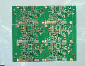
8 layer pcb thickness
With the continuous development of electronic products, the requirements for PCB are getting higher and higher. Especially for some complex electronic products, such as high-performance computers, communication equipment, etc., multi-layer boards are often needed to meet their complex wiring requirements. Among these multi-layer boards, 8-layer boards are more common. So, for the stacking structure of PCB 8-layer boards, what is the 8 layer pcb thickness

The stacked structure of PCB8-layer board usually consists of 4 inner layers and 4 outer layers. For the thickness selection of each layer, the following factors need to be considered:
- Signal integrity: The thickness of each layer will affect the signal transmission speed and impedance matching. Usually, the thickness of the inner layer will be slightly greater than the outer layer to provide better signal integrity.
- Mechanical strength: PCB8-layer board needs to withstand various forces and pressures during assembly, so the thickness of each layer also needs sufficient mechanical strength to ensure the stability of the entire board.
- Heat dissipation performance: For some high-power density electronic products, such as power amplifiers, inverters, etc., the heat dissipation performance of each layer needs to be considered. Usually, thinner inner layers and thicker outer layers are selected to improve heat dissipation performance.
Taking all the above factors into consideration, generally speaking, the following scheme can be adopted for the thickness selection of each layer of PCB 8-layer board:
Inner layer board 1: thickness 0.1mm
Inner layer board 2: thickness 0.1mm
Inner layer board 3: thickness 0.1mm
Inner layer board 4: thickness 0.1mm
Outer layer board 1: thickness 0.15mm
Outer layer board 2: thickness 0.15mm
Outer layer board 3: thickness 0.15mm
Outer layer board 4: thickness 0.15mm
Such a stacked structure can ensure signal integrity and mechanical strength while also taking into account the needs of heat dissipation performance.
Of course, the specific needs of each project may be different, so when choosing the thickness of each layer of the PCB 8-layer board, it is recommended to make a comprehensive consideration based on the actual situation and make a choice based on full communication with the PCB manufacturer.
In general, the 8 layer pcb thickness is not a fixed value, but needs to be weighed and selected according to the needs of the specific project.
Key points in design and manufacturing of 8 layer PCB thickness
When designing and manufacturing 8-layer PCBs, thickness is a key factor that directly affects the performance and reliability of the board.
First, it is crucial to understand the standard thickness range of 8-layer PCBs. Typically, the thickness of an 8-layer PCB is between 1.2 mm and 2.4 mm, depending on the design requirements and application environment. Choosing the right thickness not only helps ensure electrical performance, but also meets mechanical strength and thermal requirements.
Next, the choice of interlayer dielectric has a significant impact on PCB thickness. The thickness and dielectric constant of the interlayer dielectric material directly affect the speed and quality of signal transmission.
Commonly used dielectric materials include FR4, polyimide, etc. FR4 materials are widely used because of their good electrical properties and mechanical strength, but in high-frequency applications, low dielectric constant materials such as polyimide may be more suitable.
Therefore, when designing an 8-layer PCB, appropriate dielectric materials must be selected based on the specific application to optimize signal integrity and electrical performance.
In addition, the copper foil thickness is also an important factor affecting the total thickness of the PCB. Standard copper foil thickness is typically 1 ounce (approximately 35 microns), but thicker or thinner copper foil may be selected based on current carrying capabilities and thermal needs.
Thicker copper foil helps improve current carrying capacity and heat dissipation performance, but also increases the overall PCB thickness and manufacturing cost.
Therefore, it is necessary to weigh the relationship between electrical performance and cost during the design stage and select the most appropriate copper foil thickness.
The manufacturing process also has an important impact on the thickness of the 8-layer PCB.
The lamination process is one of the key steps in determining PCB thickness. During the lamination process, layers of materials are bonded together under high temperatures and pressures to form the final multi-layer structure.
The control of lamination pressure and temperature directly affects the tightness of the bonding between layers and the final thickness. Therefore, precise control of lamination process parameters is key to ensuring thickness consistency and quality of 8-layer PCBs.
Finally, testing and verification are important aspects to ensure that the 8-layer PCB thickness meets the design requirements. After the manufacturing is completed, the thickness measurement and quality inspection of the PCB need to be carried out using X-ray, microscope and other tools to ensure that the thickness of each layer is uniform and meets the design specifications.
Through rigorous testing and verification, problems that may arise during the manufacturing process can be discovered and corrected, ensuring the reliability and performance of the final product.
To sum up, the design and manufacturing of 8-layer PCB thickness involves multiple key factors, including interlayer dielectric selection, copper foil thickness, manufacturing process and test verification. By taking these factors into consideration, the thickness of the 8-layer PCB can be optimized to ensure its performance and reliability in a variety of applications.


