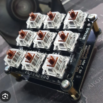
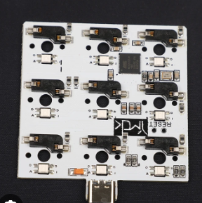
9 key pcb
Design and production guide for 9-key PCB.
When designing and making 9 key PCB, you first need to clarify its application scenarios and functional requirements. 9 key PCBs are usually used in small keyboards, control panels, or other electronic devices that require a small number of keys. Understanding these requirements helps determine circuit design, component selection, and layout planning.
Next, choosing the right circuit design software is a crucial step.
Commonly used software includes Eagle, KiCad, and Altium Designer. These software provide rich functions to help designers draw circuit diagrams, wiring, and generate Gerber files. With these tools, designers can accurately plan the location and connection of each component to ensure the stability and reliability of the circuit.
When drawing the circuit diagram, special attention should be paid to the design of the key matrix.
9-key PCBs usually adopt a 3×3 matrix layout, which can effectively reduce the number of I/O pins required. Each key is connected to a row and a column, and the state of the key is detected by scanning the row and column signals. This design not only simplifies the circuit, but also improves the accuracy of detection.
Component selection is also an important link in the design process that cannot be ignored. In addition to the keys
themselves, it is also necessary to select appropriate components such as resistors, capacitors, and diodes. The parameters of these components directly affect the performance and stability of the circuit. For example, choosing the right resistor value can ensure the accuracy of the key detection signal, while the capacitor can filter out the noise in the circuit.
After completing the circuit diagram design, enter the PCB layout stage.
Factors such as the physical size, heat dissipation and signal integrity of the components need to be considered during layout. Reasonable layout can reduce electromagnetic interference and improve the reliability of the circuit. Generally, the keys should be placed in the central area of the PCB, and other components are distributed around according to functional requirements. In addition, crossover and excessively long traces should be avoided as much as possible during wiring to reduce signal delay and interference.
Generating Gerber files is the last step in making PCBs.
Gerber files contain all the information of PCBs, including component locations, wiring, and drilling. These files will be sent to PCB manufacturers for the production of actual circuit boards. When choosing a manufacturer, factors such as its production capacity, quality control, and delivery time should be considered to ensure that the final product meets the design requirements.
In short, the design and production of 9-key PCBs involves multiple links, and each step requires careful planning and execution. From demand analysis to circuit design, to component selection and PCB layout, every detail directly affects the performance and reliability of the final product. Through reasonable design and precise production, it can be ensured that the 9-key PCB performs well in practical applications and meets various functional requirements.
How to build your own 9-key PCB keyboard
Designing and making your own 9-key PCB keyboard is a challenging and fun task.
First of all, it is crucial to understand the basic circuit design principles. Mastering these basics will help you avoid common mistakes during the design process and ensure the functionality and reliability of the final product. Next, choosing the right design software is also a key step. There are many professional PCB design software on the market, such as Eagle, KiCad, and Altium Designer, which can help you create accurate circuit diagrams and layouts.
In the design stage, determining the layout of the keyboard is the first task. The layout of the 9 keys is relatively simple, but the position and function of each key still need to be considered. You need to decide the specific purpose of each key and ensure that their arrangement is ergonomic to improve comfort and efficiency. Next, drawing the circuit diagram is the core step in the design process. The circuit diagram should include all the necessary components, such as resistors, capacitors, diodes, and microcontrollers, and clearly mark the connection relationship between them.
After completing the circuit diagram, enter the PCB layout design stage. In this stage, you need to convert the circuit diagram into an actual PCB layout. This includes determining the specific location of components on the PCB and designing circuit routing. In order to ensure the stability of signal transmission and reduce electromagnetic interference, routing design requires special attention. Using multi-layer PCBs can effectively solve these problems, but it will also increase the production cost.
After completing the PCB layout design, the next step is to generate Gerber files. These files contain all the information required for PCB manufacturing, such as copper layers, pads, silk screen layers, etc. Send the Gerber files to professional PCB manufacturers, who will produce actual PCB boards based on these files. When choosing a manufacturer, it is very important to consider its production capacity, quality control, and delivery time.
After receiving the PCB board, enter the component welding stage. Soldering is a process that requires carefulness and patience, especially for small components and dense solder joints. Using high-quality solder and soldering tools can improve the quality of welding and reduce the occurrence of welding failures. After the welding is completed, functional testing is essential. Through testing, potential problems can be discovered and fixed to ensure that each key of the keyboard can work properly.
Finally, software programming and debugging are carried out. According to the design and functional requirements of the keyboard, the corresponding firmware program is written and burned into the microcontroller. During the debugging process, using professional debugging tools and software can help you quickly locate and solve problems. At this point, a complete 9-key PCB keyboard is completed.
In short, designing and making your own 9-key PCB keyboard is a systematic project that requires the comprehensive use of circuit design, PCB layout, welding, programming and other knowledge and skills. Through continuous learning and practice, you can not only master these skills, but also enjoy the sense of accomplishment brought by DIY electronic products.


