Rigid-flex pcb fabrication
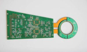
Rigid-flex PCB fabrication is the process of manufacturing printed circuit boards (PCBs) that combine both rigid and flexible materials.

Rigid-flex PCBs are used in applications where space is limited and where the board needs to bend or flex during use. The fabrication process involves several steps, including:
1. Design: The first step in the fabrication process is to design the PCB using computer-aided design (CAD) software.
2. Material selection: The next step is to select the materials for the PCB. Rigid-flex PCBs typically use a combination of rigid and flexible materials, such as FR-4 and polyimide.
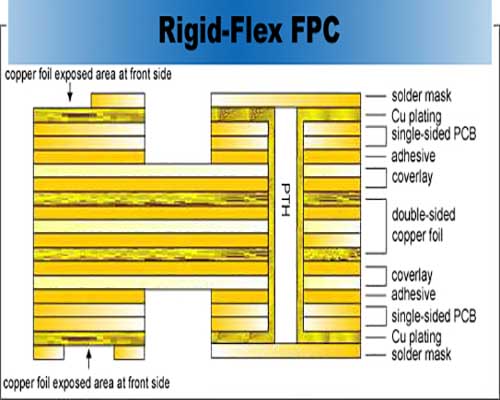
3. Layer stacking: The layers of the PCB are stacked together, with the rigid layers on the outside and the flexible layers in the middle.
4. Drilling: Holes are drilled in the PCB to allow for the insertion of components.
5. Plating: The holes are plated with copper to create electrical connections between the layers.
6. Etching: The excess copper is etched away to create the desired circuit pattern.
7. Lamination: The layers of the PCB are laminated together using heat and pressure.
8. Routing: The PCB is routed to create the final shape and size.
9. Surface finish: The PCB is finished with a surface treatment, such as gold plating, to protect the copper traces and pads.
10. Testing: The final step is to test the PCB to ensure that it functions correctly.

Overall, rigid-flex PCB fabrication is a complex process that requires specialized equipment and expertise.
The resulting PCBs are highly durable and reliable, making them ideal for use in a wide range of applications.


