4 layer pcb
1.What is 4-layer pcb
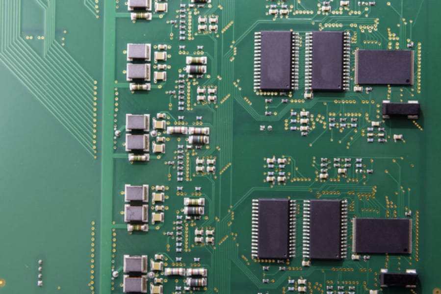
4-layer PCBs (printed circuit boards) play a vital role in modern electronic design. They not only provide higher electrical performance and better signal integrity, but also allow for more complex and compact circuit designs.
2.What is the structural composition of a 4-layer PCB?
Common substrates include FR-4, polyimide, and ceramic. FR-4 is a glass fiber reinforced epoxy resin that is widely used for its good mechanical and electrical properties.
Polyimide materials are often used in high temperature environments and flexible circuit boards due to their excellent heat resistance and flexibility.
Ceramic substrates are suitable for high frequency and high power applications due to their high thermal conductivity and low dielectric constant.
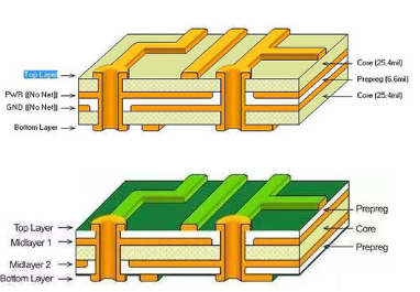
Four-layer PCBs usually consist of four conductive layers and three insulating layers. The most common structure is two signal layers sandwiched between two power layers and a ground layer.
The advantage of this structure is that it can effectively reduce electromagnetic interference (EMI) and signal crosstalk while improving the stability of the power and ground layers.
GET PCB MANUFACTURING AND ASSEMBLY QUOTE NOW!
3.What are the advantages of 4-layer PCB?
(1)higher electrical performance.
(2)better able to manage signal integrity and electromagnetic interference (EMI).
(3)effectively reduce the interference between signals and improve the stability and reliability of the circuit.
(4)helps achieve more complex circuit designs
(5) performs well in terms of space utilization
4.What are the disadvantages of 10-layer PCB?
(1)increase in cost
(2)increases the difficulty of development and production.
(3)repair and modification are also difficult
Four-layer printed circuit boards (PCBs) play a vital role in modern electronic devices.
Compared with traditional single-layer or double-layer PCBs, four-layer PCBs have significant advantages in design and application.
However, these advantages also come with some disadvantages that cannot be ignored. First, one of the main advantages of a four-layer PCB is its higher electrical performance.
Due to the multi-layer structure, four-layer PCBs are better able to manage signal integrity and electromagnetic interference (EMI).
By placing the power layer and ground layer in the inner layer respectively, the four-layer PCB can effectively reduce the interference between signals and improve the stability and reliability of the circuit. In addition, this design significantly reduces the noise level of the circuit, thereby improving the overall performance of the device.
Secondly, four-layer PCB also performs well in terms of space utilization. As electronic devices continue to be miniaturized, circuit board space becomes increasingly valuable. By increasing the number of layers, a four-layer PCB can accommodate more circuits and components in a limited space.
This not only helps achieve more complex circuit designs, but also reduces the size and weight of circuit boards to meet the lightweight and compact needs of modern electronic devices.
However, four-layer PCBs are not without drawbacks. First, its manufacturing cost is higher.
Due to the complexity of the multi-layer structure, the production process of four-layer PCB requires more materials and process steps, which directly leads to an increase in cost.
For some projects or products with limited budgets, this can become a significant constraint.
In addition, the design and manufacturing of four-layer PCBs requires a higher level of technology and experience, which also increases the difficulty of development and production.
In addition, repair and modification of four-layer PCBs are also difficult. Due to the multi-layer structure, problems with any one layer may affect the functionality of the entire circuit board.
Repairing or modifying a four-layer PCB usually requires professional equipment and technology, which not only increases the repair cost, but may also extend the repair time.
Therefore, when designing and using four-layer PCBs, special attention needs to be paid to their reliability and durability to minimize later maintenance needs.
To sum up, four-layer PCB has significant advantages in terms of electrical performance and space utilization, but its high cost and complex maintenance process also bring certain challenges.
When choosing whether to use a four-layer PCB, engineers and designers need to consider the specific needs and budget of the project and weigh its advantages and disadvantages to make the most appropriate decision.
With proper design and application, four-layer PCBs can play an important role in many high-performance and high-density electronic devices.
GET PCB AND ASSEMBLY SERVICE QUOTE NOW!
5.Application of 4-layer PCB
(1)high-performance electronic devices
(2)computer motherboards,
(3)communication equipment
(4)high-frequency circuits
(5)medical equipment
terms of applications, four-layer PCBs are widely used in high-performance electronic equipment, such as computer motherboards, communication equipment, and medical equipment.
Its high density and reliability make it the first choice in these fields. For example, in computer motherboards, four-layer PCBs can support higher processing speeds and more complex circuit designs, thereby improving overall performance.
Similarly, in communication equipment, the high signal integrity and low electromagnetic interference characteristics of four-layer PCB ensure the stability and reliability of data transmission.
In addition, the application of four-layer PCB in medical devices cannot be ignored. Medical equipment has extremely high requirements for reliability and accuracy, and the multi-layer structure and high-density design of four-layer PCB can meet these needs.
For example, in electrocardiographs and ultrasound equipment, the application of four-layer PCB ensures accurate signal transmission and stable operation of the equipment.