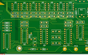
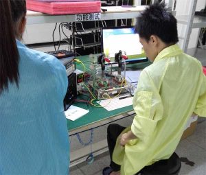
pcb testing
1. Circuit board testing method

What is the PCB board testing method? How much do you know? We have talked about what skills need to be learned about PCB design before.
This time we will expand the knowledge related to PCB boards. PCB boards are the most basic components. This time the theme is how to detect PCB boards. Let’s learn with the editor with questions in mind.
(1). When measuring voltage or testing waveforms with an oscilloscope probe, the test lead or probe should not cause a short circuit between the integrated circuit pins due to sliding.
The measurement should be performed on the peripheral printed circuit directly connected to the pins. Any momentary short circuit can easily damage the integrated circuit. When testing CMOS integrated circuits in flat packages, you must be extra careful.
(2). It is not allowed to use a soldering iron with electricity. Make sure that the soldering iron is not charged and ground the outer shell of the soldering iron. Be more careful with MOS circuits. It is safer to use a low-voltage circuit iron of 6-8V.
(3). If you need to add peripheral components to replace the damaged parts inside the integrated circuit, you should use small components and the wiring should be reasonable to avoid unnecessary parasitic coupling. In particular, you should handle the grounding terminal between the audio power amplifier integrated circuit and the preamplifier circuit.
(4) It is strictly forbidden to use instruments with grounded shells to directly test TV, audio, video and other equipment without power isolation transformers. Although most radio recorders have power transformers, when you come into contact with special TV or audio equipment, especially those with large output power or the nature of the power supply you don’t know well, you must first find out whether the chassis of the machine is energized. Otherwise, it is very easy to cause a power short circuit with the TV, audio and other equipment with energized bottom plate, affecting the integrated circuit and causing the fault to expand further.
(5) Before checking and repairing the integrated circuit, you must first be familiar with the function, internal circuit, main electrical parameters, function of each pin, normal voltage of the pin, waveform and working principle of the circuit composed of peripheral components. If the above conditions are met, then analysis and inspection will be much easier.
(6) Do not easily judge that the integrated circuit is damaged. Because most integrated circuits are directly coupled, once a circuit is abnormal, it may cause multiple voltage changes, and these changes are not necessarily caused by damage to the integrated circuit.
In addition, in some cases, when the voltage of each pin is consistent with or close to the normal value, it does not necessarily mean that the integrated circuit is good. Because some soft faults will not cause changes in DC voltage. The above is the method of PCB board detection, I hope it can help you.
GET PCB MANUFACTURING AND ASSEMBLY QUOTE NOW!
2. Main functions of PCB circuit board tester
The tester adopts circuit online testing technology, which can be used to test and analyze common faults of various small and medium-scale integrated circuit chips online or offline, and test the V/I characteristics of analog and digital devices.
• Functional test of digital chips The basic principle of the test is to detect and record the input/output state of the chip, compare the recorded state with the standard state truth table, and thus determine whether the function of the tested chip is correct.

• State test of digital chips Each digital device on the circuit board has three state characteristics after power-on: the logical state of each pin (power supply, ground, high resistance, signal, etc.), the connection relationship between the pins, and the logical relationship between input and output. When a device fails, its state characteristics generally change. The tester can extract the state characteristics of each IC device on the good circuit board, store them in the computer database, and then compare them with similar faulty circuit boards to accurately find the fault location.
• VI characteristic test analysis This test function is based on analog feature analysis technology and can be used for testing analog, digital, special devices, programmable devices, and large-scale and ultra-large-scale devices. The tester automatically extracts the characteristic curve of the measured point through the test probe or test clip, displays it on the microcomputer screen, and finally stores it in the computer. When performing special fault diagnosis, the measured VI curve is compared with the pre-stored standard curve to find the fault.
•Node voltage test Since the test object of the tester includes not only digital circuit devices but also a large number of analog circuit devices, in order to further improve the application scope of the tester, the node voltage test technology is adopted in the tester. By applying the working voltage to the object under test, the voltage response value of the test node is read by the computer, and a standard test information library is established for the operator to analyze and determine the fault location.
•Other functions In addition to the above main functions, the tester also has auxiliary test functions such as electronic manual, test development, and system self-test.
GET PCB AND ASSEMBLY SERVICE QUOTE NOW!
3. Tester composition
(1) Hardware module
The tester consists of a portable computer, a single-chip microcomputer test platform, and a test analysis and processing software. The single-chip microcomputer test platform completes the data collection of the object under test under computer control. Its basic principle block diagram is shown in Figure 1. The functions and descriptions of each part are as follows:
The single-chip microcomputer circuit mainly completes data acquisition, control, command processing, and data exchange with the computer. The MCS-51 series 8031 single-chip microcomputer is used in the tester design, 2764 is selected as the expansion ROM, and 6264 is selected as the expansion RAM. The decoding chip circuit is 74LS138. For serial communication with the computer, MCl488 and MC1489 are used to convert RS-232C level and TTL level. The single-chip microcomputer system clock frequency uses a 6MHz crystal oscillator, the communication baud rate uses 2400, and the single-chip microcomputer uses working mode 3 for serial communication.

Timer T1 is set to mode 2. Set SMOD=1, and the time constant is F3H.
The bus driver expands the single-chip microcomputer bus to improve its driving ability, and 74LS244 and 74LS245 line drivers are selected.
The drive control circuit mainly completes the control of TTL and CMOS test thresholds during the test process. A 4-layer SPST (single-pole single-throw) DG211 analog switch is selected, and the switch control is completed by the decoding circuit and the 74LS373 latch. To ensure that DG211 is in the normally open (OFF) state when it is turned on, a pull-up resistor (10kΩ) is added to the control line.
The test drive circuit applies the test input signal to the chip under test, and a micro relay is used to control the input signal. The test signal is generated by the data buffer 74ACT244. To ensure that the input current meets the design requirements, a 4-way parallel connection is adopted. To prevent damage to the device, an LC network is added for high current buffering, and a diode protection circuit is designed.
The data acquisition circuit reads the output response of the chip under test and uses a dual voltage comparator LM393 for output signal control.
It has low power consumption, high comparison accuracy, and is compatible with TTL logic. The LM393 output is connected to the 74LS373 data latch, and the comparison data is read by the single-chip microcomputer.
The voltage-driven D/A circuit completes the output of the step voltage during the VI test. The 8-bit parallel D/A converter MC1408 is used. The chip power supply voltage is +5V and -12V. The reference voltage is provided by the constant current regulator TL431. The output selects bipolar output, which is completed by the two-stage amplifier circuit LM348.
The current conversion acquisition A/D circuit implements the acquisition of test point current data. The circuit uses load resistors and differential amplifier circuit LM343 to follow the voltage of the test point and convert the current value of the test point into a voltage that can be processed by the A/D conversion circuit.
The AD7574 eight-bit successive comparison high-speed A/D conversion circuit is selected. The conversion time is 15μS and the single +5V power supply is used. The reference voltage is VREF=-8V. The input voltage range is 0~+|VREF|. The A/D conversion can be started by generating a negative pulse at the RD end of the program control chip.
(2) Software module
The tester is controlled by a portable host computer through a serial port. The single-chip test platform completes the excitation control, data acquisition and other tasks. All data analysis and processing and command control are completed by the portable host computer.
The whole set of test software consists of several main modules, including main control software, data communication software, offline test software, online functional test software, online status test software, VI characteristic test software, node voltage test software, electronic manual, test development software, system self-test software, etc.
4. Circuit online test technology
(1) Principle of online test
The basic principle of online test is that the tester provides input stimulus for the chip under test on the printed circuit board, and automatically collects and records the output response and state value of the chip under test under computer control. The computer compares all the recorded state values with the standard state truth table to judge the fault condition of the object under test.
(2) Post-drive test technology
Post-drive test technology is mainly used for online testing of digital circuits. Its essence is to inject or pull out transient large current into the input stage of the device under test (the output stage of the previous driver chip), forcing its potential to become higher or lower as required, so as to achieve the purpose of applying test stimulus to the device under test online.
In order to ensure the functional test of the device on the circuit board, the logic level of the driver device must be forced, and each pin driver must be able to absorb or output sufficient current. According to the post-drive safety standard recommended by the international protection standard document (00-53/1), the maximum drive current of the tester is designed to be 240mA, and the test time is within 200ms.
Through the experiment, the device under test can be basically isolated well, and the safety of the device under test is also ensured.


