blind buried vias
blind buried vias
1. What are blind and buried vias?
As the design of portable products is developing towards miniaturization and high density, the design difficulty of PCB is also increasing, and higher requirements are put forward for the production process of PCB. In most of the current portable products, BGA packages with a pitch below 0.65mm are all designed with blind and buried vias. So what are blind and buried vias?
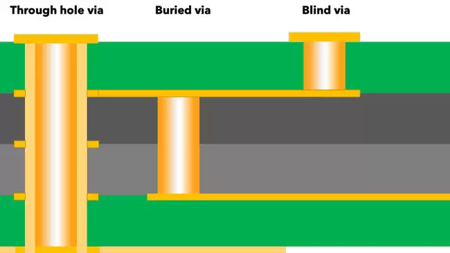
Blind vias (Laser Vias): Blind vias are vias that connect the inner layer traces of PCB with the surface traces of PCB. This hole does not penetrate the entire board.
Buried vias: Buried vias are vias that only connect the traces between the inner layers, so they cannot be seen from the surface of the PCB.
Blind and buried vias refer to a via technology that connects the inner layer traces with the surface traces in a multilayer printed circuit board (PCB) through a special processing method.
It includes two types: blind vias and buried vias. Blind vias connect the inner layer traces with the surface traces, while buried vias only connect the traces between the inner layers.
The application of blind and buried via technology has effectively improved the wiring density and reliability of the circuit board, and is an important component of modern high-density interconnect (HDI) printed circuit boards.
GET PCB MANUFACTURING AND ASSEMBLY QUOTE NOW!
2. Introduction to PCB via technology

(1) Basic knowledge of PCB vias
Via is one of the important components of multi-layer PCBs. The cost of drilling holes usually accounts for 30% to 40% of the cost of PCB board manufacturing. From the perspective of via function, it can be divided into two categories: electrical connection between layers and fixing or positioning of devices. From the perspective of process, vias are generally divided into three categories, namely blind vias, buried vias and through vias. Blind vias are located on the top and bottom surfaces of printed circuit boards and have a certain depth. They are used to connect the surface circuits and the inner circuits below. The depth of the holes usually does not exceed a certain ratio (aperture). Buried vias refer to connection holes located in the inner layers of printed circuit boards, which do not extend to the surface of the circuit board. The above two types of holes are located in the inner layers of the circuit board and are completed using the through-hole forming process before lamination. During the via formation process, several inner layers may be overlapped. The third type is called a through hole, which passes through the entire circuit board and can be used to achieve internal interconnection or as a mounting hole for components. Since through holes are easier to implement in terms of process and have lower costs, most printed circuit boards use them instead of the other two types of vias. From a design perspective, a via is mainly composed of a drill hole in the middle and a pad area around the drill hole. The size of these two parts determines the size of the via. The smaller the via, the smaller its own parasitic capacitance, which is suitable for high-speed circuits. However, the reduction in hole size also brings about an increase in cost, and is also limited by process technologies such as drilling and plating.
(2) Parasitic capacitance of vias
The parasitic capacitance of vias The via itself has stray capacitance to the parasitic ground. The main impact of the parasitic capacitance of vias on the circuit is that it prolongs the rise time of the signal and reduces the speed of the circuit. Although the effect of the rise delay caused by the parasitic capacitance of a single via is not very obvious, if vias are used multiple times in the routing to switch between layers, designers should still consider it carefully.
(3) About the parasitic inductance of vias
Vias have both parasitic capacitance and parasitic inductance. In the design of high-speed digital circuits, the harm caused by the parasitic inductance of vias is often greater than the influence of parasitic capacitance. Its parasitic series inductance will weaken the contribution of bypass capacitance and reduce the filtering effect of the entire power system. The diameter of the via has little effect on the inductance, while the length of the via has the greatest impact on the inductance. The impedance generated by the via cannot be ignored when high-frequency current passes through it. In particular, it should be noted that the bypass capacitor needs to pass through two vias when connecting the power layer and the ground layer, so the parasitic inductance of the via will increase exponentially.
(4) About the use of vias
a. Considering both cost and signal quality, choose a reasonable size of via. If necessary, consider using vias of different sizes. For example, for vias of power or ground wires, consider using larger sizes to reduce impedance, while for signal routing, use smaller vias. Of course, as the size of the via decreases, the corresponding cost will also increase.
b. The two formulas discussed above show that using thinner PCBs is beneficial to reducing the two parasitic parameters of vias.
c. Try not to change layers for signal routing on PCBs, that is, try not to use unnecessary vias.
d. Vias should be drilled near the power and ground pins, and the shorter the leads between the vias and the pins, the better. You can consider drilling multiple vias in parallel to reduce the equivalent inductance.
f. Place some grounded vias near the vias where the signal changes layers to provide the closest loop for the signal. You can even place some redundant ground vias on the PCB.
g. For high-speed PCBs with higher density, consider using micro vias.