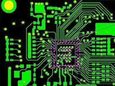
PCB board is an important electronic component, and it is the mother body of all electronic components. It has become more and more complex since the beginning of the last century. From a single layer to double layer, four layers, and multiple layers, the design is also difficult. Increasing. Because both sides of the double-layer board have wiring, understanding and mastering its wiring principles is very helpful for our design. Let’s take a look at the wiring principles of the PCB double board.
The PCB double-layer board ground wire is designed to form a grid-like frame, that is, a plurality of parallel ground wires are laid on one side of the printed board, and the other side is a vertical ground wire off the board, and then metalized vias are connected where they intersect. (The via resistance should be small).
Taking into account that each IC chip should be provided with a ground wire nearby, a ground wire is often clothed every 1 to 115 cm. Such a ground wire makes the area of the signal loop smaller, which is advantageous for reducing radiation. The ground network design method should be before the cloth signal line, otherwise, it is more difficult to achieve.
Signal line wiring principle:
After determining the reasonable layout of the components, the double-layer board shall be followed by the design of the ground copy board power cord, and then the important line—sensitive line, high-frequency line, and general line— low-frequency line. The critical lead is preferably a separate power supply, ground loop, lead and very short, so sometimes a ground wire is placed close to the signal line on the edge of the critical line to allow it to form a minimal working loop.
The principle of wiring on the top and bottom of the four-layer board is the same as that of the double-layer board. It is also the first key crystal, crystal oscillator circuit, a clock circuit, and CPU signal lines, and the principle of minimizing the circulating current area must be observed.
When the IC circuit of the printed circuit board is working, the circulation area is referred to several times in front, and its conception of differential mode radiation is actually its source. Such as the definition of differential mode radiation: the circuit operating current flows in the signal loop. This signal loop generates electromagnetic radiation. Since this current is the differential mode, the radiation generated by the signal loop is called differential mode radiation. Field strength calculation formula:
E1=K1•f2•I•A/γ
In the formula: E1—differential mode copying board The printed circuit board’s radiant field strength in the circuit space γ can be seen from the differential mode radiation formula, and its radiation field strength is proportional to the working frequency f2, circulation area A, and operating current I, such as After the operating frequency f is determined, the size of the circulating current area is a key factor that can be directly controlled in our design. At the same time, the working speed and current of the circulating current only need to satisfy the reliability, and the bigger the better, the narrower the hop along the signal’s jump edge is, and it’s harmonic. The larger the wave component, the wider the electromagnetic radiation. The higher the power, the greater the current (which has been pointed out above), which we do not expect.
The key link, if possible, is surrounded by ground wires. After the wiring of the PCB copying board is completed, all the voids can be covered with the grounding wire, but it must be noted that these covered grounding wires should be short-circuited with the low-resistance conglomerate of the large strata, so that good results can be obtained (Note: There are voids required Should meet the conditions, such as creepage distance, etc.).