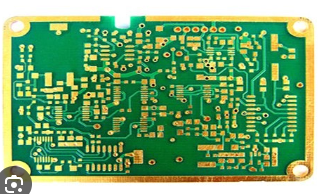
8-layer pcb stack up example
8-layer PCB stack up design example analysis
In modern electronic design, 8-layer PCB stack-up design is favored due to its complexity and high-performance characteristics.
First, it is crucial to understand the basic structure of an 8-layer PCB.
Typically, this stack-up design includes four signal layers and four power/ground layers. With this configuration, electromagnetic interference (EMI) can be effectively reduced and signal integrity can be improved.
Next, the specific functions and layout of each layer are explored.
The outermost layer is usually a signal layer, which is used to arrange critical high-frequency signal paths. The second and seventh layers that follow are usually ground layers, which help form a shielding layer to reduce the impact of external interference on the signal. In addition, the ground layer can also provide a low-impedance path to further improve signal integrity.
The third and sixth layers are usually power layers.
These layers are used to distribute different power supply voltages to meet the needs of various components. By placing the power layer on the inner side of the ground layer, a power-ground pair can be formed to reduce power supply noise and improve power supply stability. It is worth noting that the distance between the power layer and the ground layer should be as small as possible to form an efficient decoupling capacitor.
The fourth and fifth layers are usually internal signal layers.
These layers are mainly used to arrange low-frequency signals and control signals. Since these signals are less sensitive to electromagnetic interference, they can be placed in the inner layer. In addition, the wiring of the inner signal layer should be as concise as possible to reduce signal delay and crosstalk.
When designing an 8-layer PCB stackup, transitional phrases such as “In addition”, “Next”, “It is worth noting” and so on help to clearly express the functions and layout of each layer. Through reasonable interlayer configuration, the performance and reliability of the PCB can be effectively improved. For example, by arranging high-frequency signals on the outermost layer and closely following the ground layer below it, an effective shield can be formed to reduce signal radiation and interference.
Finally, the 8-layer PCB stackup design also needs to consider the manufacturing process and cost.
Although the manufacturing cost of multi-layer PCBs is high, their superior performance and reliability make them widely used in high-end electronic products. Through reasonable design and layout, the best balance between performance and cost can be found, thus achieving efficient electronic design.
In summary, the 8 layer PCB stackup design is of great significance in modern electronic design. Through reasonable interlayer configuration and layout, signal integrity and power stability can be effectively improved, and electromagnetic interference can be reduced, thus achieving high-performance electronic product design