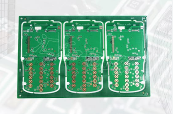
additive pcb manufacturing
Future trends and technological innovations in additive PCB manufacturing
The future trends and technological innovations of additive PCB manufacturing have attracted widespread attention in the field of electronic manufacturing.
With the continuous advancement of science and technology, the application of additive manufacturing technology in printed circuit board (PCB) production is becoming increasingly popular.
This technology not only improves production efficiency, but also significantly reduces costs.
First, additive manufacturing technology builds PCBs by adding material layer by layer, reducing material waste compared with traditional subtractive manufacturing methods.
This method is not only environmentally friendly, but also enables more complex circuit designs to meet the high performance and miniaturization needs of modern electronic products.
In addition, the advancement of additive PCB manufacturing technology is also reflected in the development of material science.
The development of new conductive and insulating materials has significantly improved the performance and reliability of additively manufactured PCBs.
For example, the application of nanomaterials not only improves electrical conductivity, but also enhances PCB durability and corrosion resistance.
Innovations in these materials provide a solid foundation for the application of additive manufacturing technology in high-end electronic products.
At the same time, the automation and intelligence of additive manufacturing technology are also constantly advancing.
The combination of advanced 3D printing technology and automated production lines makes the PCB manufacturing process more efficient and precise.
Through computer-aided design (CAD) and computer-aided manufacturing (CAM) technology, designers can design and optimize circuit boards in a virtual environment, and then directly input the design files into the 3D printer for production.
This seamless production process not only shortens the product development cycle, but also reduces the occurrence of human errors.
It is worth mentioning that additive PCB manufacturing technology also promotes the development of personalized and customized electronic products.
Traditional PCB manufacturing processes usually require a large number of molds and tools, resulting in long production cycles and high costs.
Additive manufacturing technology can quickly produce customized circuit boards according to customer needs. This flexibility makes small batch production and rapid prototyping possible, providing strong support for electronic product innovation and market response speed.
However, additive PCB manufacturing technology still faces some challenges in practical applications.
For example, how to further increase production speed and reduce costs are still issues that need to be solved.
In addition, the consistency and reliability of additively manufactured PCBs in mass production also need to be further verified.
Nevertheless, with the continuous advancement of technology and the accumulation of application experience, these problems are expected to be solved in the future.

Overall, the future of additive PCB manufacturing technology is full of opportunities and challenges. Through continuous technological innovation and application exploration, this field is expected to play an increasingly important role in the electronics manufacturing industry. Whether it is improving production efficiency, reducing costs, or achieving personalized customization, additive PCB manufacturing technology has demonstrated its huge potential and broad prospects.