Advanced assembly pcb
The latest technology trends and applications of advanced assembly PCB.
In today’s rapidly developing electronics industry, advanced assembly printed circuit board (PCB) technology is experiencing significant advancements.
These advances not only promote the miniaturization and high performance of electronic devices, but also bring new possibilities to various application fields.
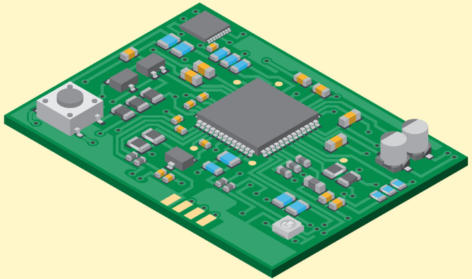
First, it’s worth noting the continued improvements in surface mount technology (SMT).
SMT allows electronic components to be mounted directly on the PCB surface, reducing the size and weight of the board.
This technological advancement makes more complex and higher-density circuit designs possible, meeting the demands for miniaturization and high performance of modern electronic devices.
At the same time, with the popularization of 5G communication technology, the demand for high-frequency and high-speed PCBs is also growing rapidly.
5G networks require higher frequencies and faster data transmission speeds, which places higher requirements on PCB materials and design.
High-frequency and high-speed PCBs use special materials, such as polytetrafluoroethylene (PTFE) and ceramic filler materials, to reduce signal loss and interference.
The application of these materials not only improves the stability of signal transmission, but also enhances the durability and reliability of the circuit board.
In addition, the progress of flexible PCB (FPCB) technology is also worthy of attention.
Flexible PCB is lightweight, bendable and durable, and is widely used in wearable devices, medical equipment, automotive electronics and other fields.
As materials science and manufacturing processes continue to develop, the performance and application range of flexible PCBs are also expanding.
For example, the latest multi-layer flexible PCB technology can realize more complex circuit designs in limited space to meet the needs of high-end electronic products.
Furthermore, advanced assembly technologies also include three-dimensional packaging (3D packaging) and system-in-package (SiP).
These technologies significantly increase circuit board integration and performance by integrating multiple chips and components into a single package.
3D packaging technology uses vertical stacking to integrate chips with different functions, thereby reducing signal transmission delay and power consumption.
System-in-package integrates multiple functional modules into one package, achieving higher system integration and smaller package size.
Finally, as environmental awareness increases, green manufacturing technology is increasingly used in advanced assembly PCBs.
The use of lead-free soldering technology and environmentally friendly materials not only reduces environmental pollution, but also improves product safety and reliability.
The application of these green technologies reflects the electronics industry’s emphasis on and commitment to sustainable development.
The process of assembling advanced PCBs involves multiple key steps, each of which is critical to ensure the quality and performance of the final product.
The design stage is the foundation of the entire process.
During this stage, engineers use computer-aided design (CAD) software to create detailed circuit diagrams and layout drawings. These drawings not only include electrical connections, but also detail the location and specifications of each component.
Once the design is completed, the next step is to generate Gerber files, which contain all the information required to manufacture the PCB.
Material selection and procurement stage.
During this stage, engineers and procurement teams work closely to select the appropriate substrate material, copper foil thickness, and other key components.
The choice of materials directly affects the performance and reliability of the PCB, so it must be done with great care.
The procurement team also needs to ensure that all components meet the design specifications and that suppliers can deliver on time.
Manufacturing stage.
The first is the graphic transfer process, which involves transferring the design pattern to the substrate. Usually using photolithography technology, the circuit pattern is accurately copied onto the copper foil through exposure and development.
Next is the etching process, which removes excess copper through chemical methods, leaving only the desired circuit pattern. After etching is completed, drilling and electroplating are carried out to create electrical connections and mounting holes.
Assembly stage.
First comes surface mount technology (SMT) assembly, which uses automated equipment to precisely place surface mount components (SMDs) on the PCB.
These components are then securely soldered to the board via reflow soldering. For PCBs that require through-hole components, through-hole technology (THT) assembly is also required, where these components are secured via wave soldering or hand soldering.
Testing and quality control
This step includes functional testing, visual inspection, and X-ray inspection to ensure that all components are properly mounted and the board is defect-free.
Functional testing verifies the performance and reliability of the PCB by simulating actual working conditions.
The quality control team also conducts sampling inspections to ensure the consistency of each batch of products.
Packaging and shipping. At this stage, the PCB is cleaned and dried to remove any residual flux and impurities.
Then, anti-static packaging is performed to prevent damage from static electricity during transportation. Once packaging is complete, the product is ready for shipment and delivered to customers.
To sum up, the latest trends in advanced assembly PCB technology cover all aspects from material selection, manufacturing process to packaging technology. The advancement of these technologies not only promotes the miniaturization and high performance of electronic devices, but also brings new possibilities to various application fields. With the continuous development of technology, we can foresee that advanced assembly PCB will play an increasingly important role in the future electronics industry.