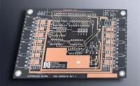
Any layer hdi pcb
Advantages Of Using HDI PCBs In Modern Electronics
High-Density Interconnect (HDI) printed circuit boards (PCBs) have become a cornerstone in the development of modern electronics, offering a multitude of advantages that cater to the ever-evolving demands of the industry.
As electronic devices continue to shrink in size while increasing in functionality, the need for more efficient and compact circuit boards has never been more critical. HDI PCBs, with their advanced design and manufacturing techniques, provide a solution that meets these stringent requirements.
One of the primary advantages of using HDI PCBs in modern electronics is their ability to support higher component density.
By utilizing finer lines and spaces, smaller vias, and capture pads, HDI technology allows for more components to be placed on both sides of the PCB. This increased component density is essential for the development of compact devices such as smartphones, tablets, and wearable technology, where space is at a premium.
Consequently, HDI PCBs enable manufacturers to create smaller, lighter, and more powerful electronic devices.
In addition to supporting higher component density, HDI PCBs also offer improved electrical performance.
The shorter distances between components and the use of microvias reduce signal loss and electromagnetic interference (EMI), leading to better signal integrity and faster signal transmission. This is particularly important in high-speed applications, such as data communication and advanced computing, where maintaining signal integrity is crucial for optimal performance. Furthermore, the reduced parasitic inductance and capacitance in HDI PCBs contribute to lower power consumption, which is a significant advantage in battery-operated devices.
Another notable benefit of HDI PCBs is their enhanced reliability.
The use of microvias and blind/buried vias in HDI designs reduces the number of through-holes, which can be potential points of failure. This results in a more robust and reliable PCB that can withstand the rigors of modern electronic applications. Additionally, the improved thermal management capabilities of HDI PCBs help dissipate heat more effectively, preventing overheating and extending the lifespan of the electronic device.
The versatility of HDI PCBs is another factor that makes them indispensable in modern electronics.
They can be used in a wide range of applications, from consumer electronics to automotive and aerospace industries. The ability to integrate multiple functions into a single, compact PCB makes HDI technology ideal for complex and high-performance applications.
Moreover, the flexibility in design and manufacturing processes allows for rapid prototyping and faster time-to-market, giving companies a competitive edge in the fast-paced electronics industry.
While the advantages of HDI PCBs are numerous, it is essential to acknowledge the challenges associated with their implementation.
The advanced manufacturing processes required for HDI technology can be more complex and costly compared to traditional PCBs. However, the long-term benefits, such as improved performance, reliability, and miniaturization, often outweigh the initial investment.
As the demand for smaller, more powerful electronic devices continues to grow, the adoption of HDI PCBs is expected to increase, driving further advancements in manufacturing techniques and cost reduction.
In conclusion, the advantages of using HDI PCBs in modern electronics are manifold, ranging from higher component density and improved electrical performance to enhanced reliability and versatility. As technology continues to advance and the demand for compact, high-performance devices grows, HDI PCBs will play an increasingly vital role in shaping the future of electronics. By embracing HDI technology, manufacturers can stay ahead of the curve, delivering innovative and reliable products that meet the ever-evolving needs of consumers and industries alike.
Key Design Considerations For HDI PCB Layout
When designing High-Density Interconnect (HDI) printed circuit boards (PCBs), several key considerations must be taken into account to ensure optimal performance and manufacturability. HDI PCBs, known for their higher wiring density per unit area compared to traditional PCBs, are essential in modern electronics where space constraints and performance demands are ever-increasing. To achieve a successful HDI PCB layout, designers must meticulously plan and execute various aspects of the design process.
First and foremost, understanding the material properties is crucial.
The choice of materials impacts the electrical performance, thermal management, and mechanical stability of the PCB. High-frequency applications, for instance, require materials with low dielectric constants and low loss tangents to minimize signal degradation. Additionally, the thermal properties of the materials must be considered to ensure efficient heat dissipation, which is vital for maintaining the reliability and longevity of the PCB.
Transitioning to the layout phase, the stack-up configuration is a critical factor.
The stack-up defines the arrangement of the various layers within the PCB, including signal layers, power planes, and ground planes. A well-designed stack-up can significantly reduce electromagnetic interference (EMI) and improve signal integrity.
It is essential to balance the number of layers to meet the design requirements while keeping manufacturing costs in check. Moreover, the use of microvias, blind vias, and buried vias in HDI PCBs allows for more efficient inter-layer connections, thereby enhancing the routing density and overall performance.
Signal integrity is another paramount consideration in HDI PCB design.
As signal speeds increase, issues such as crosstalk, reflection, and attenuation become more pronounced. To mitigate these issues, designers must carefully manage trace impedance and ensure proper termination.
Controlled impedance traces, differential pairs, and adequate spacing between high-speed signals are techniques commonly employed to maintain signal integrity. Furthermore, the placement of decoupling capacitors close to power pins helps in reducing noise and stabilizing the power supply.
Thermal management cannot be overlooked in HDI PCB design.
With components packed densely, effective heat dissipation becomes challenging yet essential. Designers must incorporate thermal vias, heat sinks, and thermal pads to facilitate heat transfer away from critical components. Additionally, the use of thermal simulation tools during the design phase can help predict and address potential thermal issues before the PCB goes into production.
Manufacturability is another key aspect that must be considered throughout the HDI PCB design process.
Designers should collaborate closely with manufacturers to understand the limitations and capabilities of the fabrication process. This includes adhering to design for manufacturability (DFM) guidelines, such as minimum trace widths, spacing, and via sizes. By doing so, designers can avoid potential issues during production and ensure a higher yield rate.
Lastly, testing and validation are integral to the HDI PCB design process.
Rigorous testing, including electrical testing, thermal cycling, and mechanical stress tests, helps in identifying and rectifying any design flaws. This step is crucial for ensuring that the final product meets the required performance standards and reliability criteria.
In conclusion, designing an HDI PCB involves a comprehensive approach that encompasses material selection, stack-up configuration, signal integrity management, thermal management, manufacturability considerations, and thorough testing. By meticulously addressing these key design considerations, designers can create high-performance, reliable, and manufacturable HDI PCBs that meet the demands of modern electronic applications.
Manufacturing Process Of HDI PCBs: A Step-By-Step Guide
High-Density Interconnect (HDI) Printed Circuit Boards (PCBs) have become a cornerstone in the electronics industry, particularly in applications requiring compact, high-performance devices.
The manufacturing process of HDI PCBs is intricate and involves several meticulous steps to ensure the final product meets stringent quality standards. Understanding this process is crucial for anyone involved in electronics design and manufacturing.
The journey begins with the selection of raw materials.
High-quality substrates, typically made from materials like FR4, are chosen for their excellent electrical insulation properties and mechanical strength. These substrates form the foundation upon which the intricate circuitry of the HDI PCB will be built. Once the substrate is prepared, the next step involves the application of a thin layer of copper foil on both sides. This copper layer will eventually form the conductive pathways of the PCB.
Following the application of the copper foil, the process moves to the creation of the circuit pattern.
This is achieved through a method known as photolithography. A photosensitive resist is applied to the copper-clad substrate, and a photomask is used to expose the desired circuit pattern onto the resist.
The exposed areas are then developed, revealing the underlying copper, which is subsequently etched away using a chemical solution. This leaves behind the precise copper traces that form the circuit.
As the circuit pattern is established, the next phase involves drilling microvias, which are tiny holes that connect different layers of the PCB.
These microvias are a defining feature of HDI PCBs, allowing for higher component density and improved electrical performance. Laser drilling is typically employed for this task due to its precision and ability to create extremely small vias.
Once the microvias are drilled, the process continues with the plating of these vias. Electrolytic plating is used to deposit a thin layer of copper inside the vias, ensuring a reliable electrical connection between the layers. This step is critical, as any defects in the plating can lead to circuit failures.
Following the plating, the PCB undergoes a series of lamination processes.
Multiple layers of the PCB are stacked and bonded together under high pressure and temperature. This creates a solid, multi-layered structure that is essential for the complex circuitry of HDI PCBs. Each layer must be perfectly aligned to ensure the integrity of the connections between them.
After lamination, the PCB is subjected to additional drilling and plating processes to create through-holes and additional vias as required by the design. These steps are similar to the initial microvia drilling and plating but are performed on the now multi-layered structure.
The next stage involves the application of a solder mask, which is a protective layer that covers the entire surface of the PCB except for the areas where components will be soldered. This mask prevents solder bridges and protects the copper traces from oxidation and other environmental factors.
Finally, the PCB undergoes surface finishing, where a thin layer of metal, such as gold or silver, is applied to the exposed copper pads. This enhances solderability and protects the pads from corrosion. The finished PCB is then subjected to rigorous testing to ensure it meets all electrical and mechanical specifications.
In conclusion, the manufacturing process of HDI PCBs is a complex and precise endeavor that requires careful attention to detail at every step. From material selection to final testing, each phase is crucial in producing a high-quality PCB that meets the demands of modern electronic devices. Understanding this process not only highlights the sophistication involved but also underscores the importance of quality control in the production of these essential components.
Comparing HDI PCBs To Traditional PCBs: What You Need To Know
When comparing High-Density Interconnect (HDI) PCBs to traditional PCBs, it is essential to understand the fundamental differences and advantages that HDI technology brings to the table.
Traditional PCBs have been the backbone of electronic devices for decades, but as technology advances, the demand for more compact, efficient, and high-performing circuits has led to the development of HDI PCBs. These advanced circuit boards offer several benefits over their conventional counterparts, making them increasingly popular in various industries.
One of the primary distinctions between HDI PCBs and traditional PCBs lies in their design and construction.
HDI PCBs are characterized by their higher wiring density per unit area, achieved through the use of finer lines and spaces, smaller vias, and capture pads.
This increased density allows for more components to be placed on a single board, which is particularly advantageous in applications where space is at a premium, such as in smartphones, tablets, and other compact electronic devices.
In contrast, traditional PCBs typically have larger traces and spaces, which can limit the number of components that can be integrated into a given area.
Moreover, HDI PCBs utilize advanced manufacturing techniques, such as laser drilling and sequential lamination, to create microvias and blind/buried vias.
These techniques enable the creation of more complex and multi-layered designs, which can significantly enhance the performance and functionality of the final product. Traditional PCBs, on the other hand, often rely on mechanical drilling, which can be less precise and may not support the same level of complexity. Consequently, HDI PCBs can offer better signal integrity and reduced signal loss, making them ideal for high-speed and high-frequency applications.
Another critical factor to consider is the reliability and durability of HDI PCBs compared to traditional PCBs.
The advanced materials and manufacturing processes used in HDI PCBs result in boards that are more robust and capable of withstanding harsh operating conditions. For instance, the use of high-quality laminates and advanced soldering techniques can improve the thermal and mechanical stability of HDI PCBs, ensuring that they perform reliably even in demanding environments. Traditional PCBs, while still reliable, may not offer the same level of performance under extreme conditions.
In addition to their technical advantages, HDI PCBs can also contribute to cost savings in the long run.
Although the initial manufacturing costs of HDI PCBs may be higher due to the advanced processes and materials involved, the overall cost of ownership can be lower. This is because HDI PCBs can reduce the need for additional components and interconnections, leading to simpler and more compact designs. Furthermore, the improved performance and reliability of HDI PCBs can result in fewer failures and less downtime, ultimately reducing maintenance and replacement costs.
It is also worth noting that the adoption of HDI PCBs can drive innovation and enable the development of new and advanced electronic products.
As technology continues to evolve, the demand for smaller, faster, and more efficient devices will only increase. HDI PCBs provide the necessary foundation for meeting these demands, allowing designers and engineers to push the boundaries of what is possible in electronic design.
In conclusion, while traditional PCBs have served the electronics industry well for many years, the advantages offered by HDI PCBs make them an attractive option for modern applications. The higher wiring density, advanced manufacturing techniques, improved reliability, and potential cost savings all contribute to the growing popularity of HDI technology. As the industry continues to evolve, it is clear that HDI PCBs will play a crucial role in shaping the future of electronic design and innovation.
Common Applications Of HDI PCBs In Various Industries
High-Density Interconnect (HDI) printed circuit boards (PCBs) have become a cornerstone in the advancement of modern electronics, finding applications across a multitude of industries. These PCBs are characterized by their higher wiring density per unit area compared to traditional PCBs, achieved through finer lines and spaces, smaller vias, and capture pads. As technology continues to evolve, the demand for more compact, efficient, and high-performing electronic devices has surged, making HDI PCBs indispensable in various sectors.
One of the primary industries benefiting from HDI PCBs is consumer electronics.
The relentless pursuit of smaller, lighter, and more powerful devices has driven manufacturers to adopt HDI technology. Smartphones, tablets, and wearable devices are prime examples where HDI PCBs are extensively used.
The compact nature of HDI PCBs allows for more components to be packed into a smaller area, enabling the production of sleek and lightweight gadgets without compromising on functionality or performance. Moreover, the enhanced electrical performance of HDI PCBs ensures that these devices can handle the high-speed data transmission required for modern applications.
Transitioning to the automotive industry, HDI PCBs play a crucial role in the development of advanced driver-assistance systems (ADAS), infotainment systems, and electric vehicles (EVs).
The automotive sector demands robust and reliable electronic systems that can withstand harsh environments and operate efficiently. HDI PCBs meet these requirements by offering improved thermal management and higher reliability. In ADAS, for instance, HDI PCBs are used in radar and camera modules, which are essential for features like lane-keeping assistance and adaptive cruise control. Similarly, in EVs, HDI PCBs are integral to battery management systems and powertrain control units, ensuring optimal performance and safety.
In the realm of telecommunications, the advent of 5G technology has further underscored the importance of HDI PCBs. The need for faster data transmission and higher bandwidth has led to the development of more sophisticated network infrastructure. HDI PCBs are employed in the construction of 5G base stations and network equipment, where their ability to support high-frequency signals and reduce signal loss is paramount. This ensures that telecommunications providers can deliver faster and more reliable services to their customers, facilitating the widespread adoption of 5G technology.
The medical industry also reaps significant benefits from HDI PCBs, particularly in the design and manufacture of medical devices. The miniaturization of medical equipment, such as portable diagnostic tools, implantable devices, and wearable health monitors, is made possible through the use of HDI technology. These devices require precise and reliable electronic components to function correctly, and HDI PCBs provide the necessary performance and reliability. For instance, in implantable devices like pacemakers, the compact size and high reliability of HDI PCBs are critical to ensuring patient safety and device efficacy.
Furthermore, the aerospace and defense sectors have long relied on HDI PCBs for their advanced electronic systems. The stringent requirements for performance, reliability, and durability in these industries make HDI PCBs an ideal choice. They are used in a variety of applications, including avionics, radar systems, and communication equipment. The ability of HDI PCBs to withstand extreme conditions and provide high-speed data processing is essential for the mission-critical operations in these fields.
In conclusion, the versatility and advanced capabilities of HDI PCBs have made them a vital component in numerous industries. From consumer electronics to automotive, telecommunications, medical, and aerospace sectors, HDI PCBs enable the development of cutting-edge technologies that drive innovation and improve the quality of life. As the demand for more compact, efficient, and high-performing electronic devices continues to grow, the significance of HDI PCBs in various applications will undoubtedly increase, solidifying their role as a key enabler of technological progress.