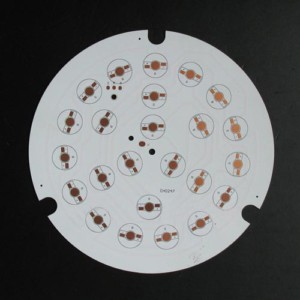
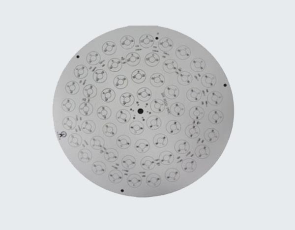
Ceramic pcb design rules
Key Considerations for Trace Width in Ceramic PCB Design
When diving into the world of ceramic PCB design, one of the most critical aspects to consider is the trace width. This might sound like a minor detail, but trust me, it can make or break your entire project. So, let’s chat about why trace width is so important and what you need to keep in mind to get it just right.
First off, let’s talk about why trace width matters.
In simple terms, the trace width is the width of the conductive paths that connect different components on your PCB. These paths are like tiny highways for electrical signals, and just like in real life, the size of the highway can affect traffic flow. If your trace is too narrow, it might not be able to handle the current, leading to overheating and potential failure. On the flip side, if it’s too wide, you could be wasting valuable space on your PCB, which is especially precious in compact designs.
Now, you might be wondering, “How do I determine the right trace width for my ceramic PCB?”
Great question! The answer depends on a few factors, including the current your traces need to carry, the material properties of the ceramic substrate, and the overall design constraints of your project. A good starting point is to use a trace width calculator, which can give you a ballpark figure based on your specific requirements. These calculators take into account factors like current, temperature rise, and the thickness of the copper layer.
Speaking of copper, let’s not forget that the material properties of your ceramic substrate also play a significant role.
Ceramic PCBs are known for their excellent thermal conductivity and mechanical strength, which can be a double-edged sword. On one hand, these properties allow for better heat dissipation, meaning you can often get away with narrower traces compared to traditional FR4 PCBs. On the other hand, the rigidity of ceramic materials means that any mistakes in trace width can be less forgiving. So, it’s crucial to get it right the first time.
Another key consideration is the manufacturing process.
Ceramic PCBs are typically produced using techniques like thick-film or thin-film deposition, each with its own set of design rules. For instance, thick-film processes might allow for wider traces but could introduce more variability in trace width. Thin-film processes, while offering higher precision, might limit the maximum trace width you can achieve. Understanding these nuances can help you make more informed decisions during the design phase.
Let’s not overlook the importance of simulation and testing.
Before you commit to a final design, it’s always a good idea to run simulations to see how your traces will perform under different conditions. Tools like SPICE (Simulation Program with Integrated Circuit Emphasis) can be invaluable for this purpose. Once you’ve got a design that looks good on paper, prototyping and testing are the next steps. This will give you a real-world sense of how your trace widths hold up under actual operating conditions.
In summary, getting the trace width right in ceramic PCB design is a balancing act that involves understanding your current requirements, leveraging the unique properties of ceramic materials, and navigating the intricacies of the manufacturing process. By paying close attention to these factors and using the right tools for simulation and testing, you can ensure that your ceramic PCB not only meets but exceeds your performance expectations. So, next time you’re working on a ceramic PCB, give those tiny highways the attention they deserve. Your project will thank you for it!
Thermal Management Strategies in Ceramic PCB Layout
When it comes to designing ceramic PCBs, one of the most critical aspects to consider is thermal management. Effective thermal management strategies can make or break the performance and longevity of your electronic devices. Ceramic PCBs, known for their excellent thermal conductivity and mechanical stability, offer unique advantages, but they also come with their own set of design rules that need to be followed to optimize thermal performance.
First and foremost, understanding the material properties of ceramic substrates is essential.
Ceramics like aluminum oxide (Al2O3) and aluminum nitride (AlN) are commonly used due to their high thermal conductivity. AlN, for instance, boasts a thermal conductivity of around 170 W/mK, which is significantly higher than traditional FR4 materials. This inherent property allows for efficient heat dissipation, but it also means that the layout must be meticulously planned to leverage this advantage fully.
One of the primary strategies in thermal management is the strategic placement of components.
High-power components should be placed in areas where heat can be most effectively dissipated. This often means positioning them near thermal vias or heat sinks. Thermal vias are essentially vertical pathways that allow heat to travel from the top layer of the PCB to the bottom layer, where it can be more easily managed. By placing high-power components near these vias, you can ensure that heat is quickly and efficiently moved away from critical areas.
Another crucial aspect is the use of thermal pads.
These are areas of exposed metal on the PCB that can be used to attach heat sinks or other cooling solutions. When designing a ceramic PCB, it’s important to ensure that these thermal pads are adequately sized and placed to maximize heat transfer. Additionally, using a thermal interface material (TIM) between the pad and the heat sink can further enhance thermal conductivity.
Trace width and thickness also play a significant role in thermal management.
Wider and thicker traces can carry more current and dissipate more heat. However, this needs to be balanced with the overall design requirements and space constraints. In some cases, it might be beneficial to use multiple layers to distribute heat more evenly across the PCB. This multi-layer approach can help in managing hotspots and ensuring a more uniform temperature distribution.
Moreover, the choice of solder mask can impact thermal performance.
While solder masks are primarily used to protect the PCB from oxidation and other environmental factors, they can also act as thermal insulators. Opting for a solder mask with higher thermal conductivity can aid in better heat dissipation. However, this is often a trade-off with other properties like electrical insulation and durability.
Thermal simulations can be an invaluable tool in the design process.
By using software to model the thermal behavior of your PCB, you can identify potential problem areas and make adjustments before going into production. These simulations can help you optimize component placement, trace routing, and the use of thermal vias and pads, ensuring that your final design is as efficient as possible.
In conclusion, effective thermal management in ceramic PCB design is a multifaceted challenge that requires careful consideration of material properties, component placement, trace design, and additional cooling solutions. By following these design rules and leveraging the unique advantages of ceramic substrates, you can create PCBs that not only perform well but also have a longer operational life. So, the next time you’re working on a ceramic PCB, remember that a little extra attention to thermal management can go a long way in ensuring your project’s success.
Via Design Best Practices for Ceramic PCBs
When it comes to designing ceramic PCBs, one of the most critical aspects to consider is the via design. Vias, those tiny holes that allow electrical connections between different layers of a PCB, play a crucial role in the overall performance and reliability of your circuit. So, let’s dive into some best practices for via design in ceramic PCBs to ensure your project is a smashing success.
First off, it’s essential to understand that ceramic PCBs are a bit different from their traditional FR4 counterparts.
Ceramic materials, like alumina or aluminum nitride, offer superior thermal conductivity and mechanical strength. However, these benefits come with their own set of challenges, particularly when it comes to via design. One of the primary concerns is the coefficient of thermal expansion (CTE). Ceramic materials have a lower CTE compared to metals like copper, which means that vias can be more prone to stress and potential failure due to thermal cycling. To mitigate this, it’s crucial to carefully consider the via size and placement.
Speaking of via size, it’s generally a good idea to keep your vias as small as possible while still meeting your current-carrying requirements.
Smaller vias reduce the risk of cracking and other mechanical issues. However, don’t go too small, as this can lead to manufacturing difficulties and increased resistance. A good rule of thumb is to aim for a via diameter that’s about 1.5 to 2 times the thickness of the PCB. This provides a good balance between mechanical stability and electrical performance.
Another important factor to consider is the aspect ratio of your vias.
The aspect ratio is the ratio of the via’s depth to its diameter. For ceramic PCBs, it’s best to keep the aspect ratio as low as possible, ideally below 10:1. Higher aspect ratios can lead to difficulties in the plating process, resulting in poor electrical connections and potential reliability issues. If you need to use higher aspect ratios, consider using filled or plugged vias to improve reliability.
Transitioning to via placement, it’s essential to avoid placing vias too close to the edges of the PCB or other critical components.
This can lead to mechanical stress and potential failure points. Instead, try to distribute your vias evenly across the board, keeping them away from high-stress areas. Additionally, it’s a good idea to use teardrop-shaped pads around your vias. This helps to reduce stress concentrations and improve the overall mechanical stability of the PCB.
Thermal management is another critical aspect of via design in ceramic PCBs.
Since ceramic materials have excellent thermal conductivity, they can effectively dissipate heat away from high-power components. However, it’s essential to ensure that your vias are designed to facilitate this heat transfer. One way to do this is by using thermal vias, which are vias specifically designed to conduct heat away from critical components. These vias should be placed directly beneath or near high-power components to maximize their effectiveness.
Finally, it’s essential to work closely with your PCB manufacturer throughout the design process.
Ceramic PCBs require specialized manufacturing techniques, and your manufacturer can provide valuable insights and recommendations to ensure your via design is optimized for both performance and manufacturability. By collaborating with your manufacturer, you can avoid potential pitfalls and ensure a smooth production process.
In conclusion, via design is a critical aspect of ceramic PCB design that requires careful consideration and attention to detail. By following these best practices, you can ensure that your vias are mechanically stable, electrically reliable, and optimized for thermal management. So, take the time to get your via design right, and you’ll be well on your way to creating a high-performance ceramic PCB that stands the test of time.
Material Selection Guidelines for High-Performance Ceramic PCBs
When it comes to designing high-performance ceramic PCBs, the choice of materials is absolutely crucial. You might be wondering why ceramic PCBs are even a thing when traditional FR4 boards seem to do the job just fine. Well, ceramic PCBs offer a host of benefits, especially in high-frequency and high-temperature applications. They provide excellent thermal conductivity, superior mechanical strength, and outstanding electrical insulation. But to truly harness these advantages, you need to be meticulous about your material selection.
First off, let’s talk about the ceramic substrate itself. Alumina (Al2O3) is the most commonly used material for ceramic PCBs.
It’s like the Swiss Army knife of ceramics—versatile, reliable, and cost-effective. Alumina offers good thermal conductivity and electrical insulation, making it a solid choice for a wide range of applications. However, if you’re dealing with extremely high temperatures or need even better thermal performance, you might want to consider aluminum nitride (AlN). AlN has a thermal conductivity that’s about ten times higher than alumina, which can be a game-changer for high-power applications.
Transitioning from the substrate to the conductive materials, the choice here can significantly impact the performance of your ceramic PCB.
Traditional copper is often used due to its excellent electrical conductivity and relatively low cost. However, if you’re looking for something that can withstand higher temperatures and offer better reliability, silver and gold are worth considering. Silver provides excellent electrical conductivity and is more resistant to oxidation than copper. Gold, while more expensive, offers the best corrosion resistance and is often used in high-reliability applications.
Now, let’s not forget about the dielectric materials. The dielectric layer in a ceramic PCB is crucial for maintaining electrical insulation between conductive layers.
Glass-based dielectrics are commonly used because they offer a good balance between performance and cost. However, for applications requiring higher dielectric strength and lower dielectric loss, you might want to look into advanced materials like barium titanate or other specialized ceramics.
Moving on to the adhesive materials, these are often overlooked but play a vital role in the overall performance of your ceramic PCB.
Epoxy-based adhesives are commonly used due to their strong bonding properties and ease of application. However, for high-temperature applications, silicone-based adhesives might be a better choice. They offer excellent thermal stability and can withstand the rigors of harsh environments.
As we delve deeper into the intricacies of material selection, it’s also essential to consider the manufacturing process.
The materials you choose must be compatible with the fabrication techniques used in ceramic PCB production. For instance, thick-film technology is often used for ceramic PCBs, and the materials must be able to withstand the high firing temperatures involved in this process. Similarly, if you’re using thin-film technology, the materials need to be compatible with the sputtering and etching processes.
In summary, selecting the right materials for high-performance ceramic PCBs is a balancing act that requires careful consideration of various factors. From the substrate and conductive materials to the dielectrics and adhesives, each component plays a crucial role in the overall performance of the PCB. By understanding the properties and limitations of each material, you can make informed decisions that will help you design a ceramic PCB that meets your specific needs. So, the next time you’re working on a high-performance application, remember that the devil is in the details, and choosing the right materials can make all the different.