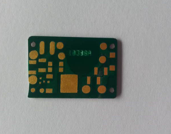
Ceramic pcb multilayer
Advantages Of Using Ceramic PCB Multilayer In High-Frequency Applications
When it comes to high-frequency applications, the choice of materials can make a world of difference. One of the standout options in this realm is ceramic PCB multilayer technology. You might be wondering, why ceramic? Well, let’s dive into the advantages and see why this material is gaining traction in the tech world.
First off, ceramic PCBs are known for their excellent thermal conductivity.
In high-frequency applications, managing heat is crucial. Traditional materials like FR4 can struggle with heat dissipation, leading to performance issues and potential damage over time. Ceramic, on the other hand, excels at spreading heat efficiently, ensuring that your components stay cool and operate optimally. This is particularly important in applications like RF (radio frequency) and microwave circuits, where even slight temperature variations can impact performance.
Moreover, ceramic PCBs offer superior electrical insulation.
High-frequency signals are sensitive to interference, and any unwanted noise can degrade the signal quality. Ceramic materials provide a stable and reliable insulating layer, minimizing the risk of signal loss or distortion. This makes them ideal for applications where signal integrity is paramount, such as in telecommunications and aerospace industries.
Another significant advantage is the mechanical strength of ceramic PCBs.
They are inherently more robust than their traditional counterparts, which means they can withstand harsh environments and physical stress. This durability is a game-changer for applications that require long-term reliability, such as in military and medical devices. You don’t want your equipment failing in critical situations, and ceramic PCBs offer that extra layer of assurance.
Transitioning to the topic of miniaturization, ceramic PCB multilayers are a boon for compact designs.
As technology advances, there’s a constant push to make devices smaller and more efficient. Ceramic PCBs can be manufactured with very fine lines and spaces, allowing for high-density interconnects. This means you can pack more functionality into a smaller footprint, which is a huge advantage in today’s world of ever-shrinking gadgets.
Furthermore, ceramic PCBs exhibit excellent chemical resistance.
In high-frequency applications, the materials used can be exposed to various chemicals and environmental conditions. Ceramic’s resistance to corrosion and chemical degradation ensures that the PCB maintains its integrity and performance over time. This is particularly beneficial in industrial and automotive applications, where exposure to harsh chemicals is common.
Let’s not forget about the high-frequency performance itself.
Ceramic materials have a low dielectric constant and low loss tangent, which means they can handle high-frequency signals with minimal loss. This is crucial for applications like satellite communications and radar systems, where maintaining signal strength and clarity is essential. The low dielectric constant also contributes to faster signal transmission, enhancing the overall performance of the device.
In addition to all these technical benefits, ceramic PCBs are also environmentally friendly.
They are made from natural materials and are generally more sustainable than traditional PCB materials. As the world moves towards greener technologies, this is an added bonus that can’t be overlooked.
In conclusion, the advantages of using ceramic PCB multilayer technology in high-frequency applications are numerous and compelling. From superior thermal management and electrical insulation to mechanical strength and miniaturization capabilities, ceramic PCBs offer a robust solution for the demands of modern high-frequency devices. Whether you’re working in telecommunications, aerospace, or any other high-tech field, ceramic PCBs can provide the performance and reliability you need to stay ahead of the curve. So, next time you’re designing a high-frequency application, consider giving ceramic PCBs a closer look—you might just find they’re the perfect fit for your needs.
Manufacturing Process Of Ceramic PCB Multilayer: A Step-By-Step Guide
If you’ve ever wondered how those intricate ceramic PCB multilayer boards are made, you’re in for a treat. These boards are the backbone of many high-tech devices, offering superior thermal management and electrical performance. Let’s dive into the step-by-step process of manufacturing these marvels of modern technology.
First things first, it all starts with the selection of the ceramic material.
Typically, alumina (Al2O3) or aluminum nitride (AlN) is chosen due to their excellent thermal and electrical properties. Once the material is selected, it’s time to prepare the ceramic substrate. This involves cutting the ceramic into the desired shape and size, ensuring it meets the specifications required for the final product.
Next up is the cleaning process.
The ceramic substrates are thoroughly cleaned to remove any impurities or contaminants that could affect the performance of the PCB. This step is crucial because even the tiniest speck of dust can lead to significant issues down the line. After cleaning, the substrates are dried to ensure they are completely free of moisture.
Now comes the fun part – creating the multilayer structure.
This is where the magic happens. The first layer of the PCB is printed using a screen-printing process. A conductive paste, usually made of silver or gold, is applied to the ceramic substrate through a stencil. This forms the circuit pattern for the first layer. The substrate is then dried and fired in a kiln to solidify the conductive paste.
Once the first layer is complete, it’s time to add the next layer.
A dielectric layer, made of a ceramic slurry, is applied over the first layer. This layer acts as an insulator between the conductive layers. The process of screen printing, drying, and firing is repeated for each subsequent layer, building up the multilayer structure one layer at a time. This step-by-step layering ensures that each layer is perfectly aligned and bonded to the previous one.
As the layers are built up, vias (vertical interconnect accesses) are created to connect the different layers electrically. These vias are formed by drilling tiny holes through the layers and filling them with conductive paste. This allows electrical signals to pass from one layer to another, creating a fully interconnected multilayer PCB.
Once all the layers are in place, the entire multilayer structure is subjected to a final firing process. This high-temperature firing ensures that all the layers are fully bonded and that the conductive paste is properly sintered. The result is a solid, robust multilayer ceramic PCB that can withstand the rigors of high-performance applications.
After firing, the PCB undergoes a series of inspections and tests to ensure it meets the required specifications.
This includes checking for any defects, measuring the electrical performance, and verifying the dimensional accuracy. Any boards that don’t meet the standards are rejected, ensuring that only the highest quality PCBs make it to the final product.
Finally, the finished ceramic PCB multilayer boards are ready for assembly.
Components are soldered onto the boards, and the final product is tested to ensure it functions as intended. And there you have it – a step-by-step guide to the manufacturing process of ceramic PCB multilayer boards. It’s a complex and meticulous process, but the end result is a high-performance PCB that’s ready to power the latest and greatest in technology.
Thermal Management Solutions With Ceramic PCB Multilayer Technology
When it comes to managing heat in electronic devices, ceramic PCB multilayer technology is a game-changer. If you’ve ever wondered why your smartphone doesn’t overheat despite being packed with powerful components, the answer often lies in the advanced thermal management solutions provided by ceramic PCBs. These multilayer boards are not just a trend; they are a necessity in today’s high-performance electronics.
First off, let’s talk about what makes ceramic PCBs so special.
Unlike traditional PCBs made from materials like FR4, ceramic PCBs are constructed from ceramic substrates such as alumina or aluminum nitride. These materials have excellent thermal conductivity, which means they can efficiently dissipate heat away from critical components. This is crucial for maintaining the performance and longevity of electronic devices, especially those that operate under high power or in harsh environments.
Now, you might be wondering, why go multilayer?
Well, multilayer ceramic PCBs take the benefits of single-layer ceramic boards and amplify them. By stacking multiple layers of ceramic and conductive materials, these PCBs can handle even more complex circuits and higher power densities. This is particularly useful in applications like aerospace, automotive, and telecommunications, where space is at a premium, and performance cannot be compromised.
One of the standout features of ceramic PCB multilayer technology is its ability to integrate various components directly into the board.
This means fewer solder joints and interconnections, which translates to higher reliability and lower risk of failure. Imagine a scenario where your car’s navigation system suddenly stops working because of a tiny solder joint failure. With ceramic multilayer PCBs, such risks are significantly minimized, ensuring that your devices are more dependable.
Moreover, the thermal management capabilities of ceramic multilayer PCBs are second to none.
These boards can operate at higher temperatures without degrading, making them ideal for high-power applications. For instance, in LED lighting systems, efficient heat dissipation is crucial to maintain brightness and extend the lifespan of the LEDs. Ceramic multilayer PCBs excel in this regard, providing a stable platform that keeps everything running smoothly.
Another advantage worth mentioning is the miniaturization potential.
As electronic devices become smaller and more powerful, the need for compact yet efficient thermal management solutions grows. Ceramic multilayer PCBs can pack a lot of functionality into a small footprint, making them perfect for modern gadgets. Whether it’s a wearable device or a high-speed communication module, these PCBs offer the flexibility and performance needed to meet the demands of cutting-edge technology.
In addition to their technical benefits, ceramic multilayer PCBs are also environmentally friendly. The materials used are generally more sustainable and have a lower environmental impact compared to traditional PCB materials. This aligns well with the growing emphasis on green technology and sustainable manufacturing practices.
So, the next time you marvel at the sleek design and robust performance of your favorite electronic device, remember that ceramic PCB multilayer technology plays a significant role behind the scenes. From enhancing thermal management to enabling miniaturization and improving reliability, these advanced PCBs are paving the way for the future of electronics. Whether you’re an engineer, a tech enthusiast, or just someone who loves their gadgets, it’s clear that ceramic multilayer PCBs are here to stay, making our devices better, faster, and more reliable than ever before.
Comparing Ceramic PCB Multilayer To Traditional PCB Materials
When it comes to printed circuit boards (PCBs), the material you choose can make a world of difference in performance, durability, and overall efficiency. While traditional PCB materials like FR4 and metal-core PCBs have been the go-to for many years, ceramic PCB multilayers are increasingly gaining traction. So, what makes ceramic PCB multilayers stand out, and how do they compare to their traditional counterparts?
First off, let’s talk about thermal management.
One of the most significant advantages of ceramic PCB multilayers is their exceptional thermal conductivity. Unlike FR4, which can struggle to dissipate heat effectively, ceramic materials like aluminum oxide and aluminum nitride excel in this area. This makes ceramic PCBs particularly suitable for high-power applications where heat dissipation is crucial. Imagine you’re working on a high-frequency device or a power LED; the last thing you want is for your PCB to overheat and fail. Ceramic PCBs can handle these thermal challenges much better, ensuring your device runs smoothly and efficiently.
Moving on to electrical performance, ceramic PCB multilayers also offer superior dielectric properties.
Traditional materials like FR4 can sometimes fall short in high-frequency applications due to their relatively high dielectric constant. Ceramic materials, on the other hand, have a lower dielectric constant, which translates to better signal integrity and reduced signal loss. This is particularly beneficial in applications like RF communication and microwave circuits, where maintaining signal quality is paramount.
Durability is another area where ceramic PCB multilayers shine.
Traditional PCBs can be prone to wear and tear, especially in harsh environments. Ceramic materials are inherently more robust and can withstand extreme conditions, including high temperatures, corrosive environments, and mechanical stress. This makes them ideal for aerospace, military, and automotive applications, where reliability is non-negotiable. Imagine deploying a satellite into space; you need a PCB that can endure the harsh conditions of outer space without compromising performance. Ceramic PCBs fit the bill perfectly.
However, it’s not all sunshine and rainbows.
One of the drawbacks of ceramic PCB multilayers is their cost. Ceramic materials are generally more expensive than traditional options like FR4. This can be a significant factor if you’re working on a budget or producing in large volumes. But, it’s worth considering the long-term benefits and potential cost savings from reduced failures and improved performance. Sometimes, investing a bit more upfront can save you a lot of headaches down the line.
Another point to consider is the manufacturing process.
Ceramic PCBs require specialized fabrication techniques, which can be more complex and time-consuming compared to traditional PCBs. This might lead to longer lead times and higher production costs. However, advancements in manufacturing technology are gradually addressing these challenges, making ceramic PCBs more accessible than ever before.
In summary, while traditional PCB materials like FR4 have their merits, ceramic PCB multilayers offer several compelling advantages, particularly in terms of thermal management, electrical performance, and durability. They are an excellent choice for high-power, high-frequency, and harsh environment applications. Yes, they come with a higher price tag and more complex manufacturing requirements, but the benefits often outweigh these drawbacks. As technology continues to evolve, we can expect ceramic PCBs to become even more prevalent, offering new possibilities for innovation and performance. So, the next time you’re designing a PCB, it might be worth giving ceramic multilayers a closer look.