Design pcb board online
Top Tools For Designing PCB Boards Online
Designing printed circuit boards (PCBs) is a critical task in the development of electronic devices, and the advent of online tools has significantly streamlined this process. These tools offer a range of functionalities that cater to both novice designers and seasoned professionals, Design pcb board online more accessible and efficient. Among the top tools for designing PCB boards online, several stand out due to their comprehensive features, user-friendly interfaces, and robust support systems.
One of the most prominent tools in this domain is EasyEDA.
This web-based platform provides a seamless experience for designing, simulating, and sharing electronic circuits. EasyEDA’s intuitive interface allows users to drag and drop components onto the design canvas, making it easy to create complex circuits. Additionally, the tool offers a vast library of components and modules, which can be integrated into designs with minimal effort. The simulation feature is particularly useful, as it enables designers to test their circuits before committing to a physical prototype, thereby saving time and resources.
Another noteworthy tool is Autodesk’s Eagle.
Known for its powerful schematic capture and PCB layout capabilities, Eagle is a favorite among professional designers. The tool’s integration with Autodesk’s suite of design software allows for a seamless transition from PCB design to 3D modeling and mechanical design. Eagle’s extensive component library and advanced routing features ensure that even the most intricate designs can be executed with precision. Moreover, the tool’s collaboration features facilitate teamwork, enabling multiple users to work on a project simultaneously.
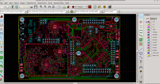
KiCad is another excellent option for online PCB design.
This open-source software offers a comprehensive suite of tools for schematic capture, PCB layout, and 3D visualization. KiCad’s flexibility and customization options make it suitable for a wide range of applications, from simple hobbyist projects to complex industrial designs. The tool’s active community of users and developers contributes to its continuous improvement, ensuring that it remains up-to-date with the latest advancements in PCB design technology.
For those seeking a more integrated approach, Altium 365 offers a cloud-based platform that combines PCB design, data management, and collaboration tools.
Altium 365’s real-time collaboration features allow team members to work together seamlessly, regardless of their physical location. The platform’s advanced data management capabilities ensure that all design files and documentation are organized and easily accessible.
Additionally, Altium 365’s integration with manufacturing partners streamlines the transition from design to production, reducing lead times and minimizing errors.
Fritzing is another valuable tool, particularly for educators and hobbyists.
This open-source software simplifies the process of designing and documenting electronic projects. Fritzing’s breadboard view allows users to create virtual prototypes that closely resemble physical breadboards, making it easier to visualize and test circuits. The tool’s schematic and PCB views provide additional layers of detail, enabling users to refine their designs before moving to production.
Fritzing’s community-driven approach ensures a wealth of resources and support for users at all skill levels.
In conclusion, the availability of online tools for PCB design has revolutionized the field, offering a range of options to suit different needs and expertise levels.
- EasyEDA,
- Eagle,
- KiCad,
- Altium 365
- Fritzing
They are among the top tools that provide comprehensive features, user-friendly interfaces, and robust support systems. By leveraging these tools, designers can create high-quality PCB boards efficiently and effectively, ultimately driving innovation in the electronics industry
Step-By-Step Guide To Creating Your First PCB Board Online
Designing a printed circuit board (PCB) online has become increasingly accessible, thanks to advancements in software and online tools.
This step-by-step guide aims to provide a comprehensive overview of the process, ensuring that even those new to PCB design can create their first board with confidence.
To begin with, the initial step involves selecting the appropriate online PCB design software
Numerous options are available, each offering unique features and varying levels of complexity. Popular choices include EasyEDA, KiCad, and Altium Designer. It is advisable to choose a platform that aligns with your skill level and project requirements. Once you have selected the software, the next step is to create a new project. This typically involves setting up the project parameters, such as the board size, layer count, and other specifications pertinent to your design.
Following the project setup, the next phase is schematic capture.
This involves creating a schematic diagram that represents the electrical connections between components. Most online PCB design tools offer a library of components that you can drag and drop onto your schematic. It is crucial to ensure that each component is correctly placed and connected, as this will directly impact the functionality of your PCB. Additionally, it is essential to label each component and connection clearly to avoid any confusion during the subsequent stages.
Once the schematic is complete, the next step is to perform a design rule check (DRC).
This automated process verifies that your schematic adheres to the predefined design rules, identifying any potential errors or issues that need to be addressed. Rectifying these errors at this stage is critical, as they can lead to significant problems during the manufacturing process.
With a verified schematic in hand, the next phase is to transition to the PCB layout.
This involves placing the components onto the board and routing the electrical connections between them. Effective component placement is vital for optimizing the board’s performance and manufacturability. It is advisable to group related components together and place them in a manner that minimizes the length of the connections. Additionally, it is important to consider factors such as heat dissipation and signal integrity during this stage.
Routing the connections, or traces, between components is a meticulous process that requires careful planning.
Most online PCB design tools offer automated routing features, but manual routing may be necessary for more complex designs. It is essential to adhere to the design rules and guidelines provided by the software to ensure that the traces are correctly routed and do not overlap or intersect inappropriately.
After completing the PCB layout, the next step is to perform a final design rule check.
This ensures that the layout adheres to all the necessary design rules and that there are no errors or issues that could impact the board’s functionality. Once the final check is complete, the design can be exported in a format suitable for manufacturing, typically Gerber files.
The final step in the process is to submit the design files to a PCB manufacturer. Many online PCB design tools offer integrated services that allow you to order your board directly from within the software. It is important to review the manufacturer’s requirements and guidelines to ensure that your design files are compatible and meet their specifications.
In conclusion, designing a PCB board online involves a series of methodical steps, from selecting the appropriate software to submitting the final design for manufacturing. By following this step-by-step guide, you can navigate the process with confidence and create a functional and reliable PCB board.
Common Mistakes To Avoid When Designing PCB Boards Online
Designing printed circuit boards (PCBs) online has become increasingly accessible, thanks to the proliferation of user-friendly software and online platforms. However, despite the convenience and advanced features these tools offer, there are common mistakes that designers, especially novices, often make. Avoiding these pitfalls is crucial for ensuring the functionality, reliability, and manufacturability of the PCB.
One frequent mistake is neglecting to adhere to design rules and guidelines.
Each PCB design software typically comes with a set of design rules that must be followed to ensure the board can be manufactured and will function correctly. These rules cover aspects such as trace width, spacing, and component placement. Ignoring these guidelines can lead to issues such as short circuits, signal interference, and even complete board failure. Therefore, it is essential to familiarize oneself with these rules and consistently apply them throughout the design process.
Another common error is improper component placement.
Components should be placed in a manner that minimizes signal path lengths and avoids crossing traces unnecessarily. Poor placement can lead to increased electromagnetic interference (EMI) and signal integrity issues. Additionally, components that generate heat should be placed in areas where they can be adequately cooled, and sensitive components should be kept away from high-power traces to prevent noise and interference. Thoughtful component placement not only enhances the board’s performance but also simplifies the routing process.
Transitioning to the next point, inadequate power distribution is another mistake that can compromise the functionality of a PCB.
Ensuring that power and ground planes are properly designed is critical for maintaining stable voltage levels and reducing noise. A common oversight is failing to provide sufficient decoupling capacitors near integrated circuits (ICs). These capacitors help to smooth out voltage fluctuations and provide a stable power supply to the ICs. Without adequate decoupling, the board may experience erratic behavior and reduced performance.
Furthermore, designers often underestimate the importance of thorough design reviews and simulations.
Relying solely on visual inspections can result in overlooked errors that could have been identified through more rigorous checks. Utilizing the simulation features available in most PCB design software can help detect issues such as signal integrity problems, thermal hotspots, and potential mechanical conflicts. Conducting these simulations before finalizing the design can save time and resources by preventing costly revisions and rework.
In addition to technical considerations, it is also vital to pay attention to the manufacturability of the PCB. This includes ensuring that the design meets the fabrication capabilities of the chosen manufacturer. For instance, some manufacturers may have limitations on minimum trace widths, hole sizes, or layer counts. Failing to account for these constraints can result in delays, increased costs, or even the inability to produce the board. Communicating with the manufacturer and understanding their capabilities can help avoid these issues.
Lastly, documentation is an often-overlooked aspect of PCB design. Comprehensive documentation, including schematics, bill of materials (BOM), and assembly drawings, is essential for the successful production and assembly of the PCB. Incomplete or unclear documentation can lead to misunderstandings, errors during manufacturing, and delays in the production process. Ensuring that all necessary information is clearly documented and easily accessible can facilitate a smoother transition from design to production.
In conclusion, while designing PCB boards online offers numerous advantages, it is crucial to be aware of and avoid common mistakes. Adhering to design rules, thoughtful component placement, proper power distribution, thorough design reviews, manufacturability considerations, and comprehensive documentation are all essential practices for creating reliable and functional PCBs. By paying attention to these details, designers can significantly improve the quality and success of their PCB projects.
Benefits Of Using Online Platforms For PCB Board Design
The advent of online platforms for PCB board design has revolutionized the electronics industry, offering numerous benefits that streamline the design process and enhance overall efficiency. One of the most significant advantages of using online platforms is the accessibility they provide.
Designers can access these tools from anywhere in the world, eliminating the need for specialized software installations on local machines. This flexibility is particularly beneficial for remote teams and individual designers who require the ability to work from various locations.
Moreover, online platforms often come equipped with a wide array of pre-designed templates and components, which can significantly reduce the time required to create a PCB board from scratch.
These resources are continually updated, ensuring that designers have access to the latest components and design standards. This feature not only accelerates the design process but also helps in maintaining consistency and reliability in the final product.
Another notable benefit is the collaborative nature of online PCB design platforms.
These tools typically offer real-time collaboration features, allowing multiple team members to work on the same project simultaneously. This capability fosters better communication and coordination among team members, leading to more efficient problem-solving and faster project completion. Additionally, version control features ensure that all changes are tracked, and previous versions can be restored if necessary, thereby minimizing the risk of errors.
Cost-effectiveness is another compelling reason to use online platforms for PCB board design.
Traditional PCB design software can be expensive, often requiring substantial upfront investment and ongoing maintenance costs. In contrast, many online platforms operate on a subscription basis or offer free versions with essential features, making them more accessible to startups, small businesses, and hobbyists. This affordability democratizes access to high-quality design tools, enabling a broader range of users to bring their electronic projects to life.
Furthermore, online PCB design platforms often integrate seamlessly with other tools and services, such as simulation software, component libraries, and manufacturing services. This integration creates a more cohesive workflow, allowing designers to move from the design phase to prototyping and production with greater ease. For instance, once a design is finalized, it can be directly sent to a manufacturer for production, reducing the time and effort required to prepare files and communicate specifications.
The user-friendly interfaces of many online PCB design platforms also contribute to their appeal.
These interfaces are designed to be intuitive, even for those who may not have extensive experience in PCB design. Tutorials, help guides, and customer support are often readily available, providing users with the assistance they need to navigate the design process effectively. This ease of use lowers the barrier to entry, encouraging more individuals to explore and engage in PCB design.
In addition to these practical benefits, online platforms also offer enhanced security features. Data encryption, secure login protocols, and regular backups ensure that sensitive design information is protected from unauthorized access and potential data loss. This level of security is crucial for businesses that handle proprietary or confidential information.
In conclusion, the benefits of using online platforms for PCB board design are manifold, ranging from increased accessibility and collaboration to cost savings and enhanced security. These platforms not only simplify the design process but also make it more efficient and accessible to a wider audience. As technology continues to advance, it is likely that online PCB design tools will become even more sophisticated, further transforming the landscape of electronic design and manufacturing.