Electronic pcb assembly
Innovations In PCB Assembly Techniques
The field of electronic PCB assembly has witnessed remarkable innovations over the past few years, driven by the relentless pursuit of efficiency, precision, and miniaturization. As technology continues to evolve, the methods and techniques used in PCB assembly have had to adapt to meet the increasing demands of modern electronic devices.
One of the most significant advancements in this area is the development of surface mount technology (SMT).
SMT has revolutionized PCB assembly by allowing components to be mounted directly onto the surface of the board, rather than being inserted into holes. This not only reduces the size and weight of the final product but also enhances the overall performance and reliability of the electronic device.
In addition to SMT, the advent of automated assembly processes has further transformed the landscape of PCB manufacturing.
Automated pick-and-place machines, for instance, have significantly increased the speed and accuracy of component placement. These machines are capable of placing thousands of components per hour with pinpoint precision, thereby reducing the likelihood of human error and ensuring a higher quality end product. Moreover, the integration of advanced vision systems in these machines allows for real-time inspection and correction, further enhancing the reliability of the assembly process.
Another noteworthy innovation in PCB assembly is the use of advanced soldering techniques.
Traditional wave soldering has largely been supplanted by reflow soldering, which offers greater control over the soldering process. Reflow soldering involves applying solder paste to the PCB, placing the components, and then heating the assembly in a reflow oven. This method ensures that the solder melts and solidifies in a controlled manner, resulting in stronger and more reliable solder joints. Additionally, selective soldering has emerged as a valuable technique for assembling complex PCBs with mixed technology components. This method allows for precise soldering of through-hole components without affecting nearby surface-mounted devices.
Furthermore, the implementation of advanced materials and coatings has played a crucial role in enhancing the durability and performance of PCBs.
For instance, the use of high-temperature laminates and specialized coatings can significantly improve the thermal management of electronic devices, thereby extending their lifespan. These materials are particularly important in applications where the PCB is exposed to harsh environmental conditions or high levels of thermal stress.
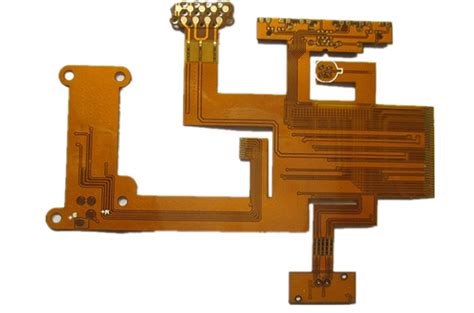
The rise of flexible and rigid-flex PCBs represents another significant innovation in the field.
These types of PCBs offer greater design flexibility and can be used in applications where traditional rigid PCBs would be impractical. Flexible PCBs, for example, can be bent and folded to fit into compact spaces, making them ideal for use in wearable devices and other miniaturized electronics. Rigid-flex PCBs, on the other hand, combine the benefits of both rigid and flexible PCBs, providing a robust yet adaptable solution for complex electronic assemblies.
Moreover, the integration of advanced testing and inspection techniques has become an integral part of the PCB assembly process.
Automated optical inspection (AOI) and X-ray inspection systems are now commonly used to detect defects and ensure the quality of the assembled PCBs. These systems can identify issues such as solder joint defects, component misalignment, and other anomalies that could compromise the performance of the final product.
In conclusion, the innovations in PCB assembly techniques have significantly enhanced the efficiency, reliability, and versatility of electronic devices. From surface mount technology and automated assembly processes to advanced soldering techniques and the use of cutting-edge materials, these advancements have paved the way for the development of increasingly sophisticated and compact electronic products. As technology continues to advance, it is likely that we will see even more groundbreaking innovations in the field of PCB assembly, further pushing the boundaries of what is possible in electronic design and manufacturing.
The Role Of Automation In PCB Manufacturing
In the ever-evolving landscape of electronics manufacturing, the role of automation in Printed Circuit Board (PCB) assembly has become increasingly pivotal. As the demand for more complex and miniaturized electronic devices grows, the need for precision, efficiency, and scalability in PCB manufacturing has never been more critical. Automation, with its myriad of technological advancements, is revolutionizing the way PCBs are assembled, offering numerous benefits that are reshaping the industry.
To begin with, automation significantly enhances the accuracy and consistency of PCB assembly.
Traditional manual assembly methods are prone to human error, which can lead to defects and inconsistencies in the final product. Automated systems, on the other hand, utilize advanced machinery and software to ensure that each component is placed with pinpoint accuracy. This level of precision is particularly crucial for modern PCBs, which often feature extremely small components and intricate designs. By minimizing errors, automation not only improves the quality of the final product but also reduces the need for costly rework and repairs.
Moreover, automation in PCB assembly leads to substantial improvements in production speed and efficiency.
Automated assembly lines can operate around the clock, significantly increasing throughput compared to manual processes. This capability is especially beneficial for high-volume production runs, where time-to-market is a critical factor. Additionally, automated systems can quickly adapt to design changes and variations in production requirements, providing manufacturers with the flexibility needed to meet the dynamic demands of the electronics market. This adaptability is further enhanced by the integration of advanced software tools that facilitate real-time monitoring and optimization of the assembly process.
Another key advantage of automation is its ability to reduce labor costs.
While the initial investment in automated equipment can be substantial, the long-term savings in labor expenses can be significant. Automated systems require fewer operators, and those that are needed can focus on higher-value tasks such as quality control and process optimization. This shift not only reduces direct labor costs but also helps address the growing shortage of skilled labor in the electronics manufacturing industry. By leveraging automation, manufacturers can maintain high levels of productivity without being constrained by labor market fluctuations.
In addition to cost savings, automation also contributes to improved workplace safety.
Manual PCB assembly often involves repetitive tasks that can lead to musculoskeletal disorders and other health issues for workers. Automated systems can perform these tasks with greater speed and precision, reducing the risk of injury and creating a safer working environment. Furthermore, automation can handle hazardous materials and processes, such as soldering, more safely than human operators, thereby minimizing exposure to potentially harmful substances.
As we look to the future, the role of automation in PCB assembly is set to expand even further with the advent of Industry 4.0 technologies.
The integration of the Internet of Things (IoT), artificial intelligence (AI), and machine learning into automated systems promises to bring new levels of intelligence and connectivity to the manufacturing process. These technologies will enable predictive maintenance, real-time data analytics, and enhanced decision-making capabilities, further driving efficiency and innovation in PCB assembly.
In conclusion, the role of automation in PCB manufacturing is multifaceted and transformative. By enhancing accuracy, increasing efficiency, reducing costs, and improving safety, automation is not only meeting the current demands of the electronics industry but also paving the way for future advancements. As technology continues to evolve, the integration of automation in PCB assembly will undoubtedly remain a cornerstone of modern electronics manufacturing, driving progress and innovation in this critical field.
Common Challenges In PCB Assembly And How To Overcome Them
Printed Circuit Board (PCB) assembly is a critical process in the manufacturing of electronic devices, involving the mounting of electronic components onto a PCB to create functional circuits. Despite advancements in technology, several common challenges persist in PCB assembly, which can impact the quality, reliability, and performance of the final product. Understanding these challenges and implementing effective strategies to overcome them is essential for ensuring successful PCB assembly.
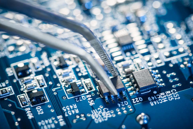
One of the primary challenges in PCB assembly is component placement accuracy.
With the increasing miniaturization of electronic components, precise placement has become more critical than ever. Misaligned components can lead to poor electrical connections, resulting in device malfunction or failure. To address this issue, manufacturers can invest in advanced pick-and-place machines equipped with high-resolution cameras and sophisticated algorithms. These machines can accurately position components on the PCB, reducing the likelihood of placement errors.
Another significant challenge is soldering defects, which can manifest as solder bridges, cold joints, or insufficient solder.
These defects can compromise the electrical integrity of the PCB, leading to intermittent connections or complete circuit failure. To mitigate soldering issues, it is crucial to maintain optimal soldering conditions, including temperature control and proper flux application. Additionally, implementing automated optical inspection (AOI) systems can help identify soldering defects early in the assembly process, allowing for timely corrective actions.
Thermal management is also a critical concern in PCB assembly, particularly for high-power applications.
Inadequate heat dissipation can cause components to overheat, leading to reduced performance or permanent damage. To overcome thermal management challenges, designers can incorporate thermal vias, heat sinks, and thermal pads into the PCB layout. Moreover, selecting components with appropriate thermal ratings and using thermal interface materials can enhance heat dissipation and ensure the longevity of the electronic device.
Electrostatic discharge (ESD) is another challenge that can adversely affect PCB assembly.
ESD can damage sensitive electronic components, resulting in latent defects that may not be immediately apparent. To prevent ESD-related issues, manufacturers should implement stringent ESD control measures, such as using ESD-safe workstations, grounding wrist straps, and anti-static packaging materials. Additionally, training personnel on ESD prevention techniques can further minimize the risk of ESD damage during the assembly process.
Component availability and supply chain disruptions pose significant challenges in PCB assembly.
The global electronics industry is often subject to fluctuations in component supply, which can lead to delays in production schedules. To mitigate the impact of supply chain disruptions, manufacturers can adopt strategies such as maintaining a buffer stock of critical components, diversifying suppliers, and establishing strong relationships with key vendors. Furthermore, designing PCBs with alternative component options can provide flexibility in sourcing and reduce dependency on single suppliers.
Lastly, ensuring compliance with industry standards and regulations is essential in PCB assembly.
Non-compliance can result in product recalls, legal penalties, and damage to the manufacturer’s reputation. To ensure compliance, manufacturers should stay updated with relevant standards, such as IPC-A-610 for electronic assemblies and RoHS for hazardous substances. Implementing robust quality control processes and conducting regular audits can help maintain adherence to these standards and ensure the production of high-quality PCBs.
In conclusion, while PCB assembly presents several challenges, adopting advanced technologies, implementing stringent quality control measures, and staying informed about industry standards can significantly enhance the assembly process. By addressing issues related to component placement, soldering defects, thermal management, ESD, supply chain disruptions, and regulatory compliance, manufacturers can improve the reliability and performance of their electronic devices, ultimately achieving greater success in the competitive electronics market.
Quality Control Measures In PCB Assembly
Quality control measures in PCB assembly are paramount to ensuring the reliability and functionality of electronic devices. As the backbone of modern electronics, printed circuit boards (PCBs) require meticulous attention to detail throughout the assembly process. This begins with the selection of high-quality materials, as the foundation of a robust PCB lies in the integrity of its components. By sourcing components from reputable suppliers, manufacturers can mitigate the risk of defects and ensure consistency in performance.
Transitioning from material selection, the next critical step involves the inspection of incoming components.
This process, often referred to as incoming quality control (IQC), involves rigorous testing and verification to confirm that each component meets specified standards. Techniques such as X-ray fluorescence (XRF) analysis and automated optical inspection (AOI) are employed to detect any discrepancies or defects. By catching issues early in the process, manufacturers can prevent faulty components from compromising the entire assembly.
Moving forward, the assembly process itself is subject to stringent quality control measures.
Surface mount technology (SMT) and through-hole technology (THT) are the two primary methods used in PCB assembly, each requiring precise placement and soldering of components. Automated machines, such as pick-and-place equipment, are calibrated to ensure accurate positioning, while solder paste inspection (SPI) systems verify the correct application of solder paste. These automated systems are complemented by manual inspections, where skilled technicians examine the boards for any anomalies that machines might miss.
As the assembly progresses, in-process quality control (IPQC) becomes crucial.
This involves continuous monitoring and testing at various stages to ensure that the assembly adheres to design specifications. Functional testing, for instance, assesses the electrical performance of the PCB, verifying that it operates as intended. Additionally, environmental stress screening (ESS) may be conducted to expose the PCB to extreme conditions, such as temperature fluctuations and vibrations, to identify potential weaknesses.
Upon completion of the assembly, final quality control (FQC) measures are implemented.
This stage includes a comprehensive inspection of the finished product, encompassing both visual and functional assessments. Automated optical inspection (AOI) systems play a significant role here, providing high-resolution images to detect any surface defects, such as solder joint issues or misaligned components. Furthermore, X-ray inspection is utilized to examine the internal structure of the PCB, ensuring that there are no hidden defects, such as voids or cracks in solder joints.
In addition to these technical measures, adherence to industry standards and certifications is essential for maintaining quality in PCB assembly.
Standards such as IPC-A-610, which outlines the acceptability of electronic assemblies, provide guidelines for workmanship and quality. Compliance with these standards not only ensures consistency but also instills confidence in customers regarding the reliability of the product.
Moreover, continuous improvement practices are integral to quality control in PCB assembly. By analyzing data from inspections and tests, manufacturers can identify trends and areas for improvement. Implementing corrective actions and refining processes based on this feedback loop helps in reducing defects and enhancing overall quality.
In conclusion, quality control measures in PCB assembly encompass a comprehensive approach, starting from material selection and extending through to final inspection. By employing a combination of automated and manual inspections, adhering to industry standards, and fostering a culture of continuous improvement, manufacturers can ensure the production of reliable and high-performing PCBs. These measures are not merely procedural but are fundamental to the integrity and success of electronic devices in an increasingly interconnected world.