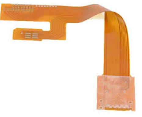
Custom flex pcb
Advantages Of Custom Flex PCB In Modern Electronics
Custom flex PCBs, or flexible printed circuit boards, have become increasingly integral to the advancement of modern electronics. These innovative components offer a multitude of advantages that cater to the evolving demands of contemporary technology.
One of the primary benefits of custom flex PCBs is their remarkable flexibility,
which allows them to be bent, folded, and twisted without compromising their functionality. This adaptability is particularly advantageous in applications where space constraints and complex geometries are prevalent, such as in wearable devices, medical implants, and compact consumer electronics.
Moreover, custom flex PCBs contribute significantly to the miniaturization of electronic devices.
By enabling the integration of multiple components onto a single, flexible substrate, these PCBs reduce the need for bulky connectors and wiring. This not only conserves space but also enhances the overall reliability of the device by minimizing potential points of failure. Additionally, the lightweight nature of flex PCBs makes them ideal for applications where weight is a critical factor, such as in aerospace and portable electronics.
Another notable advantage of custom flex PCBs is their ability to improve thermal management within electronic systems.
The materials used in flex PCBs typically exhibit superior thermal conductivity compared to traditional rigid PCBs. This characteristic facilitates more efficient heat dissipation, thereby enhancing the performance and longevity of electronic components. Furthermore, the inherent flexibility of these PCBs allows for innovative thermal management solutions, such as the incorporation of heat sinks and thermal vias in unconventional configurations.
In addition to their physical and thermal properties, custom flex PCBs offer significant benefits in terms of design versatility.
Engineers and designers can tailor these PCBs to meet specific requirements, including unique shapes, sizes, and layer configurations. This customization capability enables the development of highly specialized electronic solutions that cater to niche markets and applications. For instance, in the automotive industry, custom flex PCBs are used to create intricate sensor arrays and control systems that enhance vehicle performance and safety.
The manufacturing process of custom flex PCBs also presents several advantages.
Advanced fabrication techniques, such as additive manufacturing and laser direct structuring, allow for precise and efficient production of these PCBs. These methods not only reduce material waste but also enable rapid prototyping and iterative design improvements. Consequently, manufacturers can bring innovative products to market more quickly and cost-effectively.
Furthermore, the reliability and durability of custom flex PCBs are noteworthy.
These PCBs are designed to withstand harsh environmental conditions, including extreme temperatures, humidity, and mechanical stress. This robustness makes them suitable for use in demanding applications, such as industrial automation, military equipment, and outdoor electronics. The ability to endure such conditions ensures that devices incorporating flex PCBs maintain consistent performance and reliability over extended periods.
In conclusion, the advantages of custom flex PCBs in modern electronics are manifold. Their flexibility, miniaturization potential, thermal management capabilities, design versatility, efficient manufacturing processes, and durability collectively contribute to their growing adoption across various industries. As technology continues to advance, the role of custom flex PCBs in enabling innovative and reliable electronic solutions is poised to become even more significant.
Design Tips For Creating Efficient Custom Flex PCBs
Designing efficient custom flex PCBs requires a meticulous approach, as these flexible circuits offer unique advantages and challenges compared to traditional rigid PCBs. To begin with, understanding the specific application and environment in which the flex PCB will operate is crucial. This foundational knowledge informs decisions regarding material selection, layer configuration, and overall design strategy. For instance, applications that demand high flexibility and durability, such as wearable electronics or medical devices, necessitate the use of materials like polyimide, which offers excellent thermal stability and mechanical resilience.
Transitioning from material selection to layout considerations, it is essential to optimize the trace routing to minimize stress and potential failure points.
Flex PCBs are often subjected to bending and twisting, which can lead to mechanical fatigue. Therefore, designers should avoid sharp corners and instead use curved traces to distribute stress more evenly. Additionally, maintaining consistent trace widths and spacing helps in reducing impedance variations, which is particularly important for high-frequency signal integrity.
Another critical aspect is the stack-up configuration.
Flex PCBs can be single-sided, double-sided, or multi-layered, each offering different benefits and constraints. Single-sided flex PCBs are simpler and more cost-effective but may not provide sufficient routing space for complex designs. Double-sided and multi-layered configurations, while more expensive, offer greater routing flexibility and can accommodate more complex circuitry. When designing multi-layer flex PCBs, it is advisable to use symmetrical stack-ups to prevent warping and ensure mechanical stability.
Thermal management is another vital consideration in flex PCB design.
The thin and flexible nature of these circuits can make them more susceptible to thermal stress. Incorporating thermal vias and using materials with good thermal conductivity can help dissipate heat more effectively. Additionally, designers should consider the placement of heat-generating components and ensure adequate spacing to prevent localized hotspots.
Moving on to the mechanical design aspects, incorporating strain relief features can significantly enhance the durability of flex PCBs.
These features, such as fillets and teardrops at pad-to-trace junctions, help in distributing mechanical stress and reducing the likelihood of trace cracking. Furthermore, reinforcing areas that are subject to frequent bending with stiffeners can provide additional mechanical support and prolong the lifespan of the flex PCB.
In terms of manufacturability, it is essential to collaborate closely with the PCB manufacturer during the design phase.
Manufacturers can provide valuable insights into the limitations and capabilities of their fabrication processes, which can influence design decisions. For example, understanding the minimum bend radius that the manufacturer can achieve helps in designing flex PCBs that are both functional and manufacturable. Additionally, considering the assembly process, such as the method of component attachment and soldering, can help in designing more robust and reliable flex PCBs.
Lastly, thorough testing and validation are indispensable to ensure the reliability and performance of custom flex PCBs.
Conducting simulations to predict mechanical and thermal behavior, as well as performing physical tests under real-world conditions, can help identify potential issues early in the design process. This proactive approach not only enhances the reliability of the final product but also reduces the risk of costly redesigns and delays.
In conclusion, designing efficient custom flex PCBs involves a comprehensive understanding of material properties, layout optimization, thermal management, mechanical design, manufacturability, and rigorous testing. By carefully considering these factors and leveraging the expertise of PCB manufacturers, designers can create robust and reliable flex PCBs that meet the specific demands of their applications.
Applications Of Custom Flex PCBs In Wearable Technology
Custom flex PCBs, or flexible printed circuit boards, have become a cornerstone in the development of wearable technology. Their unique properties, such as flexibility, lightweight nature, and durability, make them ideal for applications in this rapidly evolving field. As wearable technology continues to advance, the demand for custom flex PCBs has surged, driven by their ability to meet the specific requirements of various devices.
One of the primary applications of custom flex PCBs in wearable technology is in fitness trackers.
These devices, which monitor physical activity, heart rate, and other health metrics, require components that can withstand constant movement and bending. Custom flex PCBs provide the necessary flexibility and resilience, ensuring that the device remains functional and accurate even during intense physical activities. Moreover, their lightweight nature contributes to the overall comfort and wearability of fitness trackers, making them more appealing to consumers.
In addition to fitness trackers, custom flex PCBs are also integral to the development of smartwatches.
These devices combine the functionality of traditional watches with advanced features such as notifications, GPS, and health monitoring. The compact and intricate design of smartwatches necessitates the use of flexible PCBs, which can be tailored to fit the limited space available. Furthermore, the ability to customize the PCB layout allows for the integration of various sensors and components, enhancing the overall functionality of the smartwatch.
Another significant application of custom flex PCBs is in medical wearables.
These devices, which include continuous glucose monitors, ECG monitors, and other health monitoring systems, require high reliability and precision. Custom flex PCBs can be designed to meet the stringent requirements of medical devices, ensuring accurate data collection and transmission. Additionally, their biocompatibility and resistance to environmental factors such as moisture and temperature variations make them suitable for prolonged use on the human body.
The use of custom flex PCBs extends beyond health and fitness applications.
In the realm of augmented reality (AR) and virtual reality (VR) wearables, these PCBs play a crucial role in enabling seamless integration of electronic components. AR and VR headsets require a multitude of sensors, displays, and connectivity modules, all of which need to be interconnected within a compact and ergonomic design. Custom flex PCBs provide the necessary flexibility and space-saving advantages, allowing for the creation of lightweight and comfortable headsets that enhance the user experience.
Moreover, custom flex PCBs are also finding applications in smart clothing and e-textiles.
These innovative garments incorporate electronic components such as sensors, LEDs, and communication modules, enabling functionalities like biometric monitoring, illumination, and wireless connectivity. The flexibility and durability of custom flex PCBs make them ideal for integration into fabrics, allowing for the creation of smart clothing that is both functional and comfortable to wear.
In conclusion, the applications of custom flex PCBs in wearable technology are vast and varied. Their unique properties make them indispensable in the development of devices that require flexibility, durability, and compactness. From fitness trackers and smartwatches to medical wearables, AR/VR headsets, and smart clothing, custom flex PCBs are at the forefront of innovation in wearable technology. As the demand for more advanced and versatile wearables continues to grow, the role of custom flex PCBs will undoubtedly become even more critical in shaping the future of this dynamic industry.
Cost-Effective Manufacturing Techniques For Custom Flex PCBs
Custom flexible printed circuit boards (PCBs) have become increasingly popular in various industries due to their adaptability, lightweight nature, and ability to fit into compact spaces. As demand for these versatile components grows, manufacturers are continually seeking cost-effective techniques to produce high-quality custom flex PCBs. One of the primary methods to achieve cost efficiency is through the optimization of material selection. By carefully choosing substrates and conductive materials that balance performance with affordability, manufacturers can significantly reduce production costs. Polyimide, for instance, is a commonly used substrate due to its excellent thermal stability and flexibility, while copper remains the preferred conductive material for its superior electrical properties.
In addition to material selection, advancements in manufacturing processes play a crucial role in cost reduction.
Roll-to-roll processing, for example, is a technique that allows for continuous production of flex PCBs, thereby increasing throughput and reducing labor costs. This method involves feeding a roll of flexible substrate through various stages of printing, etching, and lamination, which not only streamlines the manufacturing process but also minimizes material waste. Furthermore, the implementation of automated inspection systems ensures that defects are detected early in the production cycle, reducing the likelihood of costly rework or scrap.
Another significant factor in cost-effective manufacturing is the design optimization of custom flex PCBs.
By leveraging advanced design software, engineers can create layouts that maximize the use of available space and minimize the number of layers required. This not only reduces material costs but also simplifies the manufacturing process, leading to shorter production times and lower labor expenses. Additionally, incorporating design for manufacturability (DFM) principles ensures that the PCB design is compatible with existing manufacturing capabilities, further enhancing cost efficiency.
Moreover, collaboration between designers and manufacturers is essential for achieving cost-effective production.
Early involvement of manufacturing experts in the design phase can provide valuable insights into potential cost-saving opportunities and help avoid design choices that may lead to increased production complexity or expenses. This collaborative approach fosters a more efficient design-to-production workflow, ultimately resulting in lower overall costs.
Furthermore, economies of scale can significantly impact the cost-effectiveness of custom flex PCB manufacturing.
By producing larger quantities of PCBs, manufacturers can spread fixed costs, such as setup and tooling expenses, over a greater number of units, thereby reducing the cost per unit. Additionally, bulk purchasing of materials can lead to substantial discounts, further driving down production costs. However, it is essential to balance the benefits of economies of scale with the potential risks of overproduction and inventory management challenges.
Lastly, continuous improvement and innovation in manufacturing techniques are vital for maintaining cost-effectiveness in the long term.
Investing in research and development to explore new materials, processes, and technologies can lead to breakthroughs that further reduce production costs and enhance the performance of custom flex PCBs. For instance, the development of additive manufacturing techniques, such as 3D printing, holds promise for creating complex PCB designs with minimal material waste and reduced production times.
In conclusion, achieving cost-effective manufacturing of custom flex PCBs requires a multifaceted approach that encompasses material selection, process optimization, design efficiency, collaboration, economies of scale, and continuous innovation. By strategically addressing each of these factors, manufacturers can produce high-quality custom flex PCBs at competitive prices, meeting the growing demands of various industries while maintaining profitability.