Hdi pcb construction
Understanding The Basics Of HDI PCB Construction
High-Density Interconnect (HDI) Printed Circuit Boards (PCBs) represent a significant advancement in the field of electronics, offering enhanced performance and miniaturization capabilities. Understanding the basics of HDI PCB construction is essential for those involved in the design and manufacturing of modern electronic devices. This article aims to elucidate the fundamental aspects of HDI PCB construction, providing a comprehensive overview of the processes and technologies involved.
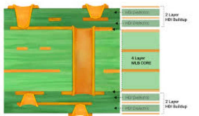
To begin with, HDI PCBs are characterized by their higher wiring density per unit area compared to traditional PCBs.
This increased density is achieved through the use of finer lines and spaces, smaller vias, and higher connection pad density. The construction of HDI PCBs typically involves multiple layers, which are interconnected using microvias. These microvias are significantly smaller than the vias used in conventional PCBs, allowing for more compact and efficient designs.
The construction process of HDI PCBs starts with the selection of appropriate materials.
High-quality substrates, such as FR4 or polyimide, are commonly used due to their excellent electrical and thermal properties. The choice of material is crucial as it directly impacts the performance and reliability of the final product. Once the substrate is selected, the next step involves the application of a thin layer of copper, which serves as the conductive material for the circuit.
Following the application of the copper layer, the next phase involves the creation of the circuit pattern.
This is typically achieved through a process known as photolithography. During photolithography, a photosensitive resist is applied to the copper layer, and the desired circuit pattern is transferred onto the resist using ultraviolet light. The exposed areas of the resist are then developed, revealing the underlying copper, which is subsequently etched away to form the circuit pattern.
Once the circuit pattern is established, the next step involves the drilling of microvias.
These microvias are created using advanced laser drilling techniques, which allow for precise and accurate hole formation. The microvias are then plated with copper to establish electrical connections between the different layers of the PCB. This process, known as via filling, is critical for ensuring the integrity and reliability of the interconnections.
After the microvias are filled, the next phase involves the lamination of the different layers.
This is achieved through a process known as sequential lamination, where each layer is individually laminated and then bonded together to form a single, cohesive structure. Sequential lamination allows for greater design flexibility and enables the creation of complex, multi-layered HDI PCBs.
Following lamination, the final steps in HDI PCB construction involve surface finishing and testing.
Surface finishing techniques, such as electroless nickel immersion gold (ENIG) or organic solderability preservative (OSP), are applied to protect the copper surfaces and enhance solderability. Rigorous testing is then conducted to ensure the functionality and reliability of the HDI PCB. This includes electrical testing, thermal cycling, and other quality assurance measures.

In conclusion, the construction of HDI PCBs involves a series of intricate and precise processes, each of which plays a critical role in determining the performance and reliability of the final product. From material selection and circuit patterning to microvia drilling and sequential lamination, each step requires careful attention to detail and advanced technological capabilities. Understanding these basics is essential for anyone involved in the design and manufacturing of high-performance electronic devices, as HDI PCBs continue to play a pivotal role in the advancement of modern electronics.
Key Materials Used In HDI PCB Manufacturing
High-Density Interconnect (HDI) printed circuit boards (PCBs) represent a significant advancement in the field of electronics, enabling the creation of more compact, efficient, and powerful devices. The construction of HDI PCBs involves the use of several key materials, each playing a crucial role in ensuring the board’s performance, reliability, and manufacturability. Understanding these materials is essential for appreciating the complexities and innovations inherent in HDI PCB manufacturing.
To begin with, the substrate material forms the foundation of any PCB, including HDI variants.
The most commonly used substrate material is FR-4, a composite made of woven fiberglass cloth with an epoxy resin binder that is flame resistant. FR-4 is favored for its excellent mechanical strength, electrical insulation properties, and thermal stability. However, for HDI PCBs, where higher performance is often required, advanced materials such as polyimide or Rogers laminates may be used. These materials offer superior thermal and electrical properties, making them suitable for high-frequency applications and environments with extreme temperature variations.
Moving on to the conductive materials, copper is the primary choice for creating the intricate circuitry on HDI PCBs.
Copper’s excellent electrical conductivity and ductility make it ideal for forming the fine traces and vias that characterize HDI designs. The copper is typically deposited onto the substrate through a process called electroplating, which ensures a uniform and reliable conductive layer. In some cases, additional surface treatments such as immersion gold or organic solderability preservatives (OSP) are applied to the copper to enhance its solderability and protect it from oxidation.
Another critical material in HDI PCB construction is the dielectric material, which insulates the conductive layers from each other.
The dielectric material must possess high electrical insulation properties while maintaining a low dielectric constant to minimize signal loss and crosstalk. Common dielectric materials used in HDI PCBs include prepregs and core materials made from epoxy resins, polyimides, or other advanced polymers. These materials are carefully selected to match the thermal expansion properties of the substrate and copper layers, ensuring the board’s structural integrity during thermal cycling.
Furthermore, the use of microvias is a defining feature of HDI PCBs, allowing for higher component density and more complex routing.
Microvias are tiny holes that connect different layers of the PCB, and their construction requires precise drilling techniques. Laser drilling is the preferred method for creating microvias due to its accuracy and ability to produce small, clean holes. The choice of laser type, such as CO2 or UV lasers, depends on the specific materials and design requirements of the HDI PCB.
Additionally, solder masks and silkscreens are essential materials in HDI PCB manufacturing.
The solder mask is a protective layer applied over the copper traces to prevent solder bridges and short circuits during the assembly process. It also provides environmental protection and improves the board’s overall durability. Silkscreens, on the other hand, are used to print component labels, logos, and other markings on the PCB, aiding in assembly and troubleshooting.
In conclusion, the construction of HDI PCBs involves a careful selection of key materials, each contributing to the board’s performance and reliability. From the substrate and conductive materials to the dielectric layers and protective coatings, every component must be meticulously chosen and precisely applied. This intricate interplay of materials and processes underscores the sophistication of HDI PCB manufacturing, enabling the development of cutting-edge electronic devices that continue to push the boundaries of technology.
Advantages Of HDI PCBs In Modern Electronics
High-Density Interconnect (HDI) Printed Circuit Boards (PCBs) have become a cornerstone in the advancement of modern electronics, offering numerous advantages that cater to the ever-evolving demands of the industry. One of the primary benefits of HDI PCBs is their ability to support higher component density. This is achieved through the use of microvias, blind vias, and buried vias, which allow for more intricate and compact designs. Consequently, HDI PCBs enable the development of smaller, lighter, and more efficient electronic devices, which is particularly advantageous in sectors such as consumer electronics, telecommunications, and medical devices.
In addition to supporting higher component density, HDI PCBs also enhance electrical performance.
The shorter signal paths and reduced parasitic effects associated with HDI technology result in improved signal integrity and faster signal transmission. This is crucial in high-speed applications where maintaining signal quality is paramount. Furthermore, the use of advanced materials and manufacturing techniques in HDI PCBs contributes to better thermal management, ensuring that devices operate reliably even under demanding conditions.
Another significant advantage of HDI PCBs is their ability to facilitate the integration of advanced features and functionalities.
The increased routing density and layer count in HDI designs allow for the incorporation of more complex circuits and components, such as processors, memory modules, and sensors. This level of integration is essential for the development of sophisticated electronic systems, such as smartphones, tablets, and wearable devices, which require a high degree of functionality within a limited space.
Moreover, HDI PCBs offer greater design flexibility, enabling engineers to create innovative and customized solutions tailored to specific applications.
The use of laser drilling technology in the fabrication of microvias allows for precise and accurate placement of vias, which is essential for achieving optimal performance in high-density designs. Additionally, the ability to stack multiple layers in HDI PCBs provides designers with more options for routing and interconnecting components, leading to more efficient and reliable designs.
The reliability and durability of HDI PCBs are also noteworthy.
The advanced manufacturing processes and materials used in HDI construction result in PCBs that are more resistant to mechanical stress, thermal cycling, and environmental factors. This ensures that HDI-based devices have a longer lifespan and can withstand the rigors of everyday use. Furthermore, the improved thermal management capabilities of HDI PCBs help prevent overheating and extend the operational life of electronic components.
Cost-effectiveness is another important consideration when evaluating the advantages of HDI PCBs.
While the initial investment in HDI technology may be higher compared to traditional PCBs, the long-term benefits often outweigh the costs. The ability to integrate more functionality into a smaller footprint can lead to significant savings in terms of materials, assembly, and testing. Additionally, the enhanced performance and reliability of HDI PCBs can reduce the need for costly repairs and replacements, further contributing to overall cost savings.
In conclusion, the advantages of HDI PCBs in modern electronics are manifold, encompassing higher component density, improved electrical performance, advanced feature integration, design flexibility, reliability, durability, and cost-effectiveness. As the demand for more compact, efficient, and sophisticated electronic devices continues to grow, HDI PCBs are poised to play an increasingly vital role in meeting these challenges and driving innovation in the industry.
Step-By-Step Guide To HDI PCB Design And Fabrication
High-Density Interconnect (HDI) Printed Circuit Boards (PCBs) represent a significant advancement in the field of electronics, offering enhanced performance and miniaturization. The design and fabrication of HDI PCBs involve a series of meticulous steps, each crucial to achieving the desired functionality and reliability. This step-by-step guide aims to elucidate the process, ensuring a comprehensive understanding of HDI PCB construction.
To begin with, the initial phase of HDI PCB design involves defining the requirements and specifications.
This includes determining the board’s size, layer count, and the type of components to be used. Once the specifications are established, the next step is schematic design. This involves creating a detailed circuit diagram that outlines the electrical connections between components. Advanced software tools are typically employed to facilitate this process, ensuring accuracy and efficiency.
Following the schematic design, the layout design phase commences.
This step is critical as it involves placing components on the board and routing the electrical connections. Given the high-density nature of HDI PCBs, this phase requires careful consideration of signal integrity, power distribution, and thermal management. Designers often use specialized software to optimize the layout, ensuring minimal signal interference and efficient use of space.
Once the layout design is finalized, the next step is to generate the necessary files for fabrication.
These files, often in Gerber format, contain detailed information about the board’s layers, including copper traces, solder masks, and silkscreens. Additionally, a Bill of Materials (BOM) is created, listing all the components required for assembly.
Transitioning to the fabrication phase, the first step involves preparing the substrate material, typically a high-quality laminate such as FR4 or a more advanced material like Rogers. The substrate is then coated with a thin layer of copper, which will form the conductive traces. The next step is to apply a photoresist layer to the copper-clad substrate. This photoresist is then exposed to ultraviolet light through a photomask, which defines the pattern of the traces.
After exposure, the board undergoes a development process where the unexposed photoresist is removed, revealing the copper traces. The exposed copper is then etched away using a chemical solution, leaving behind the desired trace pattern. Following etching, the remaining photoresist is stripped off, and the board is cleaned to remove any residual chemicals.
The next phase involves drilling microvias, which are small holes that connect different layers of the PCB.
These microvias are typically created using laser drilling technology, which offers high precision and accuracy. Once the microvias are drilled, they are plated with copper to establish electrical connections between layers.
Subsequently, the board undergoes a series of additional processes, including the application of solder masks and silkscreens.
The solder mask is a protective layer that prevents solder bridges during component assembly, while the silkscreen provides labels and markings for component placement.
Finally, the board is subjected to electrical testing to ensure all connections are intact and there are no short circuits or open circuits. Once the board passes these tests, it is ready for assembly, where components are soldered onto the board using techniques such as Surface Mount Technology (SMT) or Through-Hole Technology (THT).
In conclusion, the construction of HDI PCBs is a complex and intricate process that requires careful planning, precise execution, and rigorous testing. By following these steps, designers and manufacturers can produce high-performance PCBs that meet the demanding requirements of modern electronic devices.