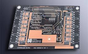
Hdi pcb type
Advantages Of HDI PCB type In Modern Electronics
High-Density Interconnect (HDI) Printed Circuit Boards (PCBs) have become a cornerstone in the advancement of modern electronics, offering numerous advantages that cater to the ever-evolving demands of the industry. As electronic devices continue to shrink in size while increasing in functionality, the need for more efficient and compact circuit boards has never been more critical. HDI PCBs address this need by providing a platform that supports higher component density, improved electrical performance, and enhanced reliability.
One of the primary advantages of HDI PCBs is their ability to accommodate a higher density of components.
This is achieved through the use of microvias, finer lines and spaces, and smaller capture pads, which allow for more components to be placed on a single board. Consequently, this leads to a reduction in the overall size and weight of the electronic device. For instance, smartphones, tablets, and wearable devices have all benefited from the miniaturization made possible by HDI technology. By enabling more compact designs, HDI PCBs contribute to the development of sleeker, more portable electronic products.
In addition to their compact size, HDI PCBs offer superior electrical performance.
The shorter signal paths and reduced parasitic effects inherent in HDI designs result in faster signal transmission and lower signal loss. This is particularly advantageous in high-speed and high-frequency applications, where signal integrity is paramount. As a result, HDI PCBs are commonly used in advanced computing systems, telecommunications equipment, and high-performance consumer electronics. The improved electrical performance not only enhances the overall functionality of the device but also contributes to energy efficiency, which is a critical consideration in today’s environmentally conscious market.
Another significant benefit of HDI PCBs is their enhanced reliability.
The use of microvias and buried vias in HDI designs reduces the number of through-hole vias, which are potential points of failure in traditional PCBs. This reduction in through-hole vias minimizes the risk of mechanical stress and thermal expansion, leading to a more robust and durable circuit board. Furthermore, the advanced manufacturing processes used in HDI PCB production, such as laser drilling and sequential lamination, ensure higher precision and consistency, further contributing to the reliability of the final product. This increased reliability is particularly important in applications where failure is not an option, such as in medical devices, aerospace, and automotive electronics.
Moreover, HDI PCBs offer greater design flexibility, allowing engineers to create more complex and innovative electronic products.
The ability to incorporate multiple layers and advanced interconnect techniques enables the integration of various functionalities within a single board. This flexibility is essential in the development of cutting-edge technologies, such as Internet of Things (IoT) devices, where multiple sensors, processors, and communication modules need to be seamlessly integrated. By providing a versatile platform for design, HDI PCBs empower engineers to push the boundaries of what is possible in modern electronics.
In conclusion, the advantages of HDI PCBs in modern electronics are manifold. Their ability to support higher component density, improved electrical performance, enhanced reliability, and greater design flexibility makes them an indispensable component in the development of advanced electronic devices. As the demand for smaller, faster, and more reliable electronics continues to grow, HDI PCBs will undoubtedly play a crucial role in shaping the future of the industry.
Key Design Considerations For HDI PCBs
High-Density Interconnect (HDI) printed circuit boards (PCBs) have become increasingly prevalent in modern electronics due to their ability to support complex designs and high-performance applications. As the demand for smaller, faster, and more efficient electronic devices continues to grow, understanding the key design considerations for HDI PCBs is essential for engineers and designers. These considerations encompass various aspects, including material selection, layer stack-up, via technology, signal integrity, thermal management, and manufacturability.
To begin with, material selection plays a crucial role in the performance and reliability of HDI PCBs.
The choice of substrate material affects the board’s electrical properties, thermal performance, and mechanical stability. Common materials used in HDI PCBs include FR-4, polyimide, and high-frequency laminates. Each material has its own set of characteristics, and the selection should be based on the specific requirements of the application. For instance, high-frequency laminates are preferred for RF and microwave applications due to their low dielectric loss and stable dielectric constant.
Moving on to layer stack-up, the configuration of the layers in an HDI PCB is critical for achieving the desired electrical performance and mechanical strength.
HDI PCBs typically feature multiple layers, including signal layers, power and ground planes, and dielectric layers. The arrangement of these layers must be carefully planned to minimize signal interference, reduce crosstalk, and ensure proper power distribution. Additionally, the use of microvias, blind vias, and buried vias in the layer stack-up allows for higher component density and more efficient routing of signals.
Via technology is another important consideration in HDI PCB design.
Vias are used to establish electrical connections between different layers of the PCB. In HDI PCBs, microvias are commonly used due to their small size and ability to connect closely spaced components. Microvias can be laser-drilled or mechanically drilled, with laser drilling being the preferred method for its precision and ability to create smaller vias. Furthermore, the use of stacked and staggered vias can enhance the routing flexibility and reduce the overall board size.
Signal integrity is a paramount concern in HDI PCB design, especially for high-speed applications. Ensuring signal integrity involves minimizing signal loss, reflection, and crosstalk. This can be achieved through careful impedance control, proper trace routing, and the use of differential pairs for high-speed signals. Additionally, the placement of decoupling capacitors and the design of power and ground planes play a significant role in maintaining signal integrity.
Thermal management is another critical aspect of HDI PCB design.
As electronic devices become more compact and powerful, effective heat dissipation becomes essential to prevent overheating and ensure reliable operation. Thermal vias, heat sinks, and thermal pads are commonly used to manage heat in HDI PCBs. Moreover, the selection of materials with high thermal conductivity can further enhance the board’s ability to dissipate heat.
Lastly, manufacturability is a key consideration that should not be overlooked.
The complexity of HDI PCBs can pose challenges during the manufacturing process. Therefore, it is important to collaborate with experienced PCB manufacturers and consider design for manufacturability (DFM) guidelines. This includes ensuring proper spacing between components, avoiding overly complex via structures, and selecting materials that are compatible with standard manufacturing processes.
In conclusion, designing HDI PCBs requires careful consideration of various factors, including material selection, layer stack-up, via technology, signal integrity, thermal management, and manufacturability. By addressing these key considerations, engineers and designers can create high-performance, reliable, and efficient HDI PCBs that meet the demands of modern electronic applications.
Manufacturing Process Of HDI PCBs
High-Density Interconnect (HDI) Printed Circuit Boards (PCBs) represent a significant advancement in the field of electronics manufacturing, offering enhanced performance and miniaturization capabilities. The manufacturing process of HDI PCBs is intricate and involves several critical steps, each contributing to the overall functionality and reliability of the final product. Understanding this process is essential for appreciating the complexity and precision required in producing these advanced circuit boards.
The journey begins with the selection of the base material, typically a high-quality laminate that provides the necessary mechanical and thermal properties.
This material serves as the foundation upon which the intricate circuitry will be built. Once the base material is chosen, the next step involves the application of a photoresist layer. This light-sensitive material is essential for defining the circuit patterns on the board. Through a process known as photolithography, the photoresist is exposed to ultraviolet light through a mask that contains the desired circuit design. The exposed areas of the photoresist harden, while the unexposed areas remain soft and can be washed away, revealing the underlying material.
Following the photolithography process, the board undergoes etching, where chemical solutions are used to remove the unwanted copper, leaving behind the precise circuit patterns. This step is crucial for ensuring the accuracy and integrity of the circuitry. After etching, the board is thoroughly cleaned to remove any residual chemicals and debris.
The next phase involves drilling microvias, which are tiny holes that connect different layers of the PCB.
These microvias are a defining feature of HDI PCBs, allowing for higher component density and improved electrical performance. Laser drilling is commonly used for this purpose due to its precision and ability to create extremely small vias. Once the microvias are drilled, they are plated with copper to establish electrical connections between the layers.
Subsequently, the board undergoes a series of lamination processes.
During lamination, multiple layers of the PCB are bonded together under heat and pressure, forming a single, cohesive unit. This step is repeated several times, depending on the complexity and layer count of the HDI PCB. Each lamination cycle is followed by additional drilling and plating to ensure proper interlayer connectivity.
After the lamination process, the board is subjected to further photolithography and etching steps to define additional circuit patterns on the outer layers.
This iterative process allows for the creation of highly complex and dense circuitry, characteristic of HDI PCBs. Once the outer layers are completed, the board undergoes surface finishing, where a protective coating is applied to prevent oxidation and enhance solderability. Common surface finishes include Electroless Nickel Immersion Gold (ENIG) and Organic Solderability Preservative (OSP).
The final stages of the manufacturing process involve solder mask application, silkscreen printing, and electrical testing.
The solder mask is a protective layer that covers the entire board, except for the areas where components will be soldered. Silkscreen printing adds labels and markings to the board for component identification and assembly guidance. Electrical testing is conducted to verify the functionality and integrity of the circuitry, ensuring that the HDI PCB meets the required specifications and performance standards.
In conclusion, the manufacturing process of HDI PCBs is a meticulous and multi-faceted endeavor that demands precision and expertise. From material selection and photolithography to drilling, lamination, and final testing, each step plays a vital role in producing high-performance circuit boards that power modern electronic devices. The advancements in HDI PCB technology continue to drive innovation in the electronics industry, enabling the development of smaller, faster, and more efficient products.
Applications Of HDI PCBs In Various Industries
High-Density Interconnect (HDI) Printed Circuit Boards (PCBs) have revolutionized the electronics industry with their advanced capabilities and compact design. These PCBs are characterized by their higher wiring density per unit area compared to traditional PCBs, achieved through finer lines and spaces, smaller vias, and capture pads. As a result, HDI PCBs are increasingly being adopted across various industries, each leveraging their unique advantages to enhance performance and innovation.
In the consumer electronics sector, HDI PCBs are indispensable due to their ability to support miniaturization while maintaining high performance.
Smartphones, tablets, and wearable devices are prime examples where HDI technology is utilized to pack more functionality into smaller, sleeker designs. The compact nature of HDI PCBs allows for more components to be placed on both sides of the board, facilitating the integration of advanced features such as high-resolution cameras, powerful processors, and extended battery life within a limited space. Consequently, consumer electronics manufacturers can deliver cutting-edge products that meet the growing demand for multifunctional and portable devices.
Transitioning to the automotive industry, HDI PCBs play a crucial role in the development of modern vehicles, particularly in the realm of advanced driver-assistance systems (ADAS) and infotainment systems
. The automotive sector requires robust and reliable electronic components that can withstand harsh environments and operate efficiently. HDI PCBs meet these requirements by offering enhanced thermal management and improved signal integrity, which are essential for the seamless operation of complex electronic systems. For instance, HDI technology enables the integration of multiple sensors, cameras, and communication modules within ADAS, thereby enhancing vehicle safety and driving experience.
Moreover, the medical industry has also embraced HDI PCBs, recognizing their potential to drive innovation in medical devices and diagnostic equipment.
The miniaturization capabilities of HDI PCBs are particularly beneficial in the development of wearable medical devices, such as glucose monitors and cardiac monitors, which require compact and reliable electronic components. Additionally, HDI PCBs are used in sophisticated imaging equipment, including MRI and CT scanners, where precision and reliability are paramount. The ability to incorporate high-density interconnects ensures that these medical devices can deliver accurate diagnostics and monitoring, ultimately improving patient care and outcomes.
Furthermore, the aerospace and defense industries have found HDI PCBs to be invaluable in the design and manufacture of advanced electronic systems.
These sectors demand high-performance, lightweight, and durable components that can operate under extreme conditions. HDI PCBs meet these stringent requirements by providing superior electrical performance and mechanical strength. They are used in a wide range of applications, from avionics and communication systems to missile guidance and radar systems. The compact and reliable nature of HDI PCBs ensures that aerospace and defense equipment can perform critical functions with high precision and reliability.
In addition to these industries, HDI PCBs are also making significant contributions to the telecommunications sector.
The rapid expansion of 5G networks and the increasing demand for high-speed data transmission have necessitated the use of advanced PCB technologies. HDI PCBs support the high-frequency signals required for 5G applications, ensuring efficient and reliable communication. Their ability to handle complex routing and high-speed signals makes them ideal for use in network infrastructure, including base stations and data centers.
In conclusion, the applications of HDI PCBs across various industries underscore their versatility and importance in driving technological advancements. From consumer electronics and automotive to medical, aerospace, defense, and telecommunications, HDI PCBs provide the foundation for developing innovative, high-performance, and reliable electronic systems. As technology continues to evolve, the role of HDI PCBs in shaping the future of electronics is set to become even more significant.