Multilayer pcb layout
Best Practices For Multilayer PCB Layout Design
Designing multilayer printed circuit boards (PCBs) is a complex task that requires meticulous attention to detail and adherence to best practices to ensure optimal performance and reliability.
One of the fundamental principles in multilayer PCB layout design is the strategic placement of components.
Proper component placement not only facilitates efficient routing but also minimizes signal interference and electromagnetic interference (EMI). It is advisable to place high-speed components close to each other to reduce the length of high-speed signal paths, thereby minimizing potential signal integrity issues.
Transitioning from component placement, another critical aspect is the layer stack-up configuration.
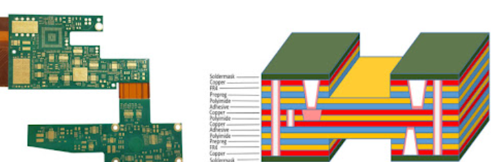
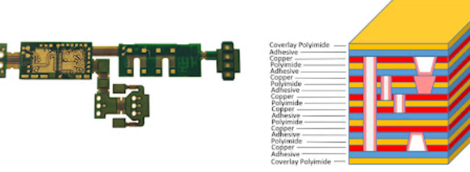
A well-thought-out layer stack-up can significantly enhance the electrical performance of the PCB. Typically, a multilayer PCB consists of alternating layers of signal and power/ground planes. The ground planes act as reference planes, providing a return path for signals and reducing EMI. It is essential to ensure that signal layers are adjacent to ground planes to maintain signal integrity and reduce crosstalk. Additionally, the symmetry of the stack-up should be maintained to prevent warping during the manufacturing process.
Moving on to routing, it is crucial to follow specific guidelines to ensure signal integrity and minimize EMI.
Differential pairs should be routed together with consistent spacing to maintain impedance control. Moreover, high-speed signals should be routed on internal layers between ground planes to shield them from external noise. It is also important to avoid sharp bends in traces, as they can cause signal reflections and impedance discontinuities. Instead, use curved or 45-degree angled traces to maintain signal integrity.
In addition to routing, via placement and management play a significant role in multilayer PCB design.
Vias are used to connect different layers of the PCB, but excessive use of vias can lead to signal degradation and increased manufacturing costs. Therefore, it is advisable to minimize the number of vias and strategically place them to ensure efficient signal flow. Blind and buried vias can be used to connect internal layers without affecting the outer layers, thereby optimizing the available routing space.
Power distribution is another critical consideration in multilayer PCB design.
A well-designed power distribution network ensures that all components receive a stable and noise-free power supply. To achieve this, it is essential to use wide power traces and planes to reduce voltage drops and maintain a low impedance path. Decoupling capacitors should be placed close to the power pins of integrated circuits to filter out noise and provide a stable power supply.
Thermal management is also a vital aspect of multilayer PCB design.
High-power components can generate significant heat, which needs to be dissipated to prevent damage and ensure reliable operation. Thermal vias, heat sinks, and thermal pads can be used to enhance heat dissipation. Additionally, the placement of components should be optimized to ensure even heat distribution across the PCB.
Finally, thorough design rule checks (DRCs) and electrical rule checks (ERCs) should be performed to identify and rectify any potential issues before manufacturing.
These checks help ensure that the design adheres to the specified constraints and standards, thereby reducing the risk of errors and rework.
In conclusion, designing a multilayer PCB requires careful consideration of various factors, including component placement, layer stack-up, routing, via management, power distribution, and thermal management. By adhering to best practices and leveraging advanced design tools, engineers can create reliable and high-performance multilayer PCBs that meet the stringent requirements of modern electronic applications.
Common Mistakes To Avoid In Multilayer PCB Layout
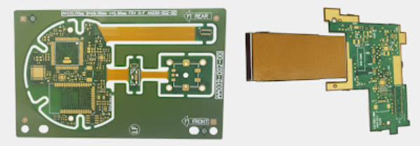
Designing multilayer printed circuit boards (PCBs) is a complex task that requires meticulous attention to detail. One of the most common mistakes in multilayer PCB layout is improper layer stack-up. The layer stack-up is crucial for signal integrity, thermal management, and overall board performance. Designers often overlook the importance of a well-planned stack-up, leading to issues such as signal crosstalk and electromagnetic interference (EMI). To avoid these problems, it is essential to carefully plan the arrangement of signal, power, and ground layers, ensuring that high-speed signals are adequately shielded and that return paths are minimized.
Another frequent error is inadequate power distribution network (PDN) design.
A poorly designed PDN can result in voltage drops, noise, and even component failure. To mitigate these risks, designers should use multiple power and ground planes to provide a low-impedance path for current flow. Additionally, decoupling capacitors should be strategically placed near power pins to filter out noise and stabilize the voltage supply. Failing to do so can compromise the performance and reliability of the entire PCB.
Thermal management is another critical aspect that is often neglected in multilayer PCB design.
Components that generate significant heat need to be properly managed to prevent overheating and ensure longevity. Designers should incorporate thermal vias, heat sinks, and adequate spacing between components to facilitate heat dissipation. Ignoring thermal considerations can lead to hot spots, which can degrade the performance of the PCB and potentially cause permanent damage.
Signal integrity issues are also a common pitfall in multilayer PCB layout.
High-speed signals are particularly susceptible to problems such as reflection, crosstalk, and signal attenuation. To maintain signal integrity, designers should pay close attention to trace impedance, routing length, and the proximity of traces to each other. Differential pairs should be routed together with consistent spacing to minimize skew, and impedance-controlled traces should be used to match the characteristic impedance of the transmission line. Neglecting these factors can result in data corruption and communication errors.
Component placement is another area where mistakes frequently occur.
Poor component placement can lead to longer trace lengths, increased EMI, and difficulty in assembly. To optimize component placement, designers should group related components together and place them in a logical sequence that minimizes trace lengths and crossovers. Additionally, components should be oriented in a way that facilitates efficient routing and assembly. Overlooking these considerations can complicate the manufacturing process and increase the likelihood of defects.
Lastly, insufficient design rule checks (DRCs) can lead to a multitude of issues in multilayer PCB layout.
DRCs are essential for verifying that the design adheres to manufacturing constraints and industry standards. Skipping or inadequately performing DRCs can result in design flaws that are only discovered during manufacturing or testing, leading to costly rework and delays. Therefore, it is imperative to thoroughly perform DRCs and address any violations before finalizing the design.
In conclusion, avoiding common mistakes in multilayer PCB layout requires careful planning and attention to detail. By properly managing layer stack-up, power distribution, thermal considerations, signal integrity, component placement, and design rule checks, designers can create robust and reliable PCBs. Taking the time to address these critical aspects will not only enhance the performance of the PCB but also ensure a smoother manufacturing process and a higher-quality end product.
Advanced Techniques For Optimizing Multilayer PCB Layout
Multilayer printed circuit boards (PCBs) have become indispensable in modern electronics, offering enhanced performance and compactness. As devices become more sophisticated, the need for advanced techniques to optimize multilayer PCB layout becomes paramount
One of the primary considerations in multilayer PCB design is the strategic placement of components.
Proper component placement not only ensures efficient use of space but also minimizes signal interference and enhances thermal management. By carefully positioning high-speed components and sensitive analog circuits, designers can mitigate potential issues related to electromagnetic interference (EMI) and crosstalk.
Transitioning from component placement, another critical aspect is the layer stack-up configuration.
The arrangement of signal, power, and ground layers significantly impacts the overall performance of the PCB. A well-thought-out stack-up can reduce EMI, improve signal integrity, and facilitate better power distribution. Typically, designers use a symmetrical stack-up to maintain mechanical stability and reduce warping during the manufacturing process. Additionally, incorporating dedicated ground planes adjacent to signal layers can provide a low-impedance return path, thereby enhancing signal integrity.
Moving forward, the routing of traces is another area where advanced techniques can make a substantial difference. High-speed signals require careful routing to avoid issues such as signal reflection and impedance mismatch. Differential pairs, commonly used for high-speed data transmission, should be routed with consistent spacing and length to maintain signal integrity. Moreover, designers should avoid sharp angles and instead use smooth, gradual curves to minimize signal degradation. Utilizing microvias and blind/buried vias can also help in managing complex routing requirements without compromising the board’s performance.
In addition to routing, power distribution is a crucial factor in multilayer PCB design.
Ensuring a stable and efficient power supply to all components is essential for reliable operation. Power planes should be designed to minimize voltage drops and noise. Using multiple power and ground planes can help in achieving a low-impedance power distribution network. Furthermore, decoupling capacitors should be strategically placed close to power pins of integrated circuits to filter out noise and provide a stable power supply.
Thermal management is another vital consideration in optimizing multilayer PCB layout.
As electronic devices become more powerful, they generate more heat, which needs to be effectively dissipated to prevent damage and ensure longevity. Designers can use thermal vias to transfer heat from hot components to other layers or to a heat sink. Additionally, spreading heat-generating components across the board and using copper pours can help in distributing heat more evenly.
Signal integrity analysis is an advanced technique that can significantly enhance the performance of multilayer PCBs.
By simulating the behavior of signals within the PCB, designers can identify potential issues such as signal reflection, crosstalk, and ground bounce. Tools like time-domain reflectometry (TDR) and eye diagram analysis can provide valuable insights into the signal quality and help in making necessary adjustments to the design.
Finally, collaboration and communication among the design team are essential for optimizing multilayer PCB layout.
Regular reviews and discussions can help in identifying potential issues early in the design process and ensure that all aspects of the design are aligned with the project requirements. Utilizing design rule checks (DRC) and adhering to industry standards can further enhance the reliability and manufacturability of the PCB.
In conclusion, optimizing multilayer PCB layout requires a comprehensive approach that encompasses strategic component placement, careful layer stack-up configuration, meticulous trace routing, efficient power distribution, effective thermal management, and thorough signal integrity analysis. By employing these advanced techniques, designers can create high-performance, reliable, and compact PCBs that meet the demands of modern electronic devices.
The Role Of Signal Integrity In Multilayer PCB Layout
In the realm of multilayer PCB (Printed Circuit Board) design, signal integrity plays a pivotal role in ensuring the optimal performance and reliability of electronic devices. As electronic systems become increasingly complex, the demand for high-speed data transmission and miniaturization has necessitated the use of multilayer PCBs. These advanced boards, which consist of multiple layers of conductive material separated by insulating layers, offer numerous advantages, including enhanced electrical performance and reduced electromagnetic interference (EMI). However, achieving these benefits requires meticulous attention to signal integrity throughout the design process.
Signal integrity refers to the quality and reliability of electrical signals as they travel through a PCB.
In multilayer PCB layouts, maintaining signal integrity is crucial because any degradation can lead to data corruption, timing errors, and overall system malfunction. One of the primary factors affecting signal integrity is impedance control. Impedance, the resistance to the flow of alternating current, must be carefully managed to ensure that signals are transmitted without distortion. This is particularly important in high-speed circuits where even minor impedance mismatches can cause significant signal reflections and loss.
To achieve proper impedance control, designers must consider the geometry of the PCB traces, the dielectric properties of the insulating materials, and the spacing between traces
By carefully selecting these parameters, it is possible to create transmission lines with consistent impedance, thereby minimizing signal reflections and ensuring signal integrity. Additionally, the use of ground planes and power planes in multilayer PCBs helps to provide a stable reference voltage and reduce noise, further enhancing signal integrity.
Another critical aspect of signal integrity in multilayer PCB layout is the management of crosstalk.
Crosstalk occurs when a signal in one trace induces an unwanted signal in an adjacent trace, leading to interference and potential data errors. To mitigate crosstalk, designers can employ techniques such as increasing the spacing between traces, using differential pairs, and incorporating shielding. Differential pairs, which consist of two complementary signals traveling in close proximity, can significantly reduce crosstalk by canceling out noise. Shielding, on the other hand, involves placing grounded conductive layers between signal layers to block electromagnetic interference.
Moreover, the placement and routing of components on a multilayer PCB can have a profound impact on signal integrity.
Strategic component placement can minimize the length of critical signal paths, reducing the potential for signal degradation. Additionally, careful routing of traces can help to avoid sharp bends and vias, which can introduce impedance discontinuities and signal reflections. By adhering to best practices in component placement and trace routing, designers can ensure that signals are transmitted with minimal distortion.
Thermal management is another factor that intersects with signal integrity in multilayer PCB design.
Excessive heat can affect the electrical properties of materials and lead to signal degradation. Therefore, designers must consider thermal management techniques such as the use of thermal vias, heat sinks, and proper airflow to maintain signal integrity under varying operating conditions.
In conclusion, signal integrity is a fundamental consideration in the design of multilayer PCBs. By carefully managing impedance, mitigating crosstalk, optimizing component placement and trace routing, and addressing thermal management, designers can ensure that their multilayer PCB layouts deliver reliable and high-performance electronic systems. As technology continues to advance, the importance of signal integrity in multilayer PCB design will only grow, underscoring the need for meticulous attention to detail and adherence to best practices in the field.