Multilayer pcb thickness
Understanding The Importance Of Multilayer PCB Thickness In Modern Electronics
In the realm of modern electronics, the significance of multilayer printed circuit board (PCB) thickness cannot be overstated. As electronic devices become increasingly complex and compact, the demand for efficient, reliable, and high-performance PCBs has surged. Multilayer PCBs, which consist of multiple layers of conductive material separated by insulating layers, are at the forefront of this technological evolution. Understanding the importance of multilayer PCB thickness is crucial for engineers and designers striving to optimize the performance and reliability of electronic devices.
To begin with, the thickness of a multilayer PCB directly influences its electrical performance.
Thicker PCBs can accommodate more layers, which allows for more intricate and dense circuit designs. This is particularly important in applications requiring high-speed signal transmission and minimal signal loss. The additional layers provide more routing options, reducing the need for long, convoluted traces that can degrade signal integrity. Consequently, a well-designed multilayer PCB with appropriate thickness can significantly enhance the overall performance of an electronic device.
Moreover, the mechanical strength of a PCB is closely tied to its thickness.
Thicker PCBs are inherently more robust and less prone to warping or bending, which is essential for maintaining the structural integrity of the board during manufacturing, assembly, and operation. This is especially critical in applications subjected to harsh environmental conditions or mechanical stress, such as automotive, aerospace, and industrial electronics. By selecting the appropriate thickness, designers can ensure that the PCB can withstand these challenges without compromising its functionality.
In addition to electrical performance and mechanical strength, thermal management is another critical aspect influenced by PCB thickness.
As electronic components become more powerful, they generate more heat, which must be effectively dissipated to prevent overheating and potential failure. Thicker PCBs can incorporate additional thermal vias and copper planes, which enhance heat dissipation and improve the overall thermal performance of the board. This is particularly important in high-power applications, where efficient thermal management is essential for maintaining the reliability and longevity of the device.
Furthermore, the manufacturing process and cost considerations are also impacted by PCB thickness.
Thicker PCBs generally require more material and longer processing times, which can increase production costs. However, the benefits of improved performance, reliability, and thermal management often outweigh these additional costs. It is essential for designers to strike a balance between the desired performance characteristics and the associated manufacturing expenses. By carefully considering the specific requirements of the application, designers can select the optimal PCB thickness that meets both performance and budgetary constraints.
In conclusion, the thickness of a multilayer PCB plays a pivotal role in determining the electrical performance, mechanical strength, thermal management, and manufacturing considerations of modern electronic devices. As technology continues to advance, the demand for high-performance, reliable, and compact PCBs will only grow. By understanding the importance of multilayer PCB thickness and its impact on various aspects of electronic design, engineers and designers can make informed decisions that enhance the overall performance and reliability of their products. This knowledge is indispensable in the ever-evolving landscape of modern electronics, where the quest for innovation and excellence drives continuous improvement and development.
How To Choose The Right Multilayer PCB Thickness For Your Project
Choosing the right multilayer PCB thickness for your project is a critical decision that can significantly impact the performance, reliability, and manufacturability of your electronic device. The process involves a careful consideration of various factors, including electrical performance, mechanical strength, thermal management, and manufacturing constraints. Understanding these elements will help you make an informed decision that aligns with your project’s specific requirements.
To begin with, electrical performance is a primary consideration when selecting the thickness of a multilayer PCB.
Thicker boards can support higher current-carrying capacity, which is essential for power-intensive applications. Conversely, thinner boards are often preferred for high-frequency applications due to their lower inductance and capacitance, which can enhance signal integrity. Therefore, it is crucial to evaluate the electrical demands of your project to determine the appropriate PCB thickness.
In addition to electrical performance, mechanical strength is another vital factor.
Thicker PCBs generally offer greater rigidity and durability, making them suitable for applications that require robust physical support. For instance, in automotive or industrial environments where the PCB may be subjected to mechanical stress or vibration, a thicker board can provide the necessary structural integrity. On the other hand, thinner PCBs are more flexible and can be advantageous in applications where space constraints are a concern, such as in compact consumer electronics.
Thermal management is also a key aspect to consider.
Thicker PCBs can dissipate heat more effectively due to their larger thermal mass, which is beneficial for high-power applications that generate significant amounts of heat. Efficient thermal management is crucial to prevent overheating and ensure the longevity of electronic components. Therefore, if your project involves high-power circuits, opting for a thicker PCB can help in maintaining optimal operating temperatures.
Manufacturing constraints and cost implications are equally important when choosing the right multilayer PCB thickness.
Thicker PCBs can be more challenging to manufacture, requiring specialized equipment and processes, which can increase production costs and lead times. Additionally, the availability of materials and the capabilities of your chosen PCB manufacturer should be taken into account. It is advisable to consult with your manufacturer early in the design process to understand their capabilities and limitations, ensuring that your design can be produced efficiently and cost-effectively.
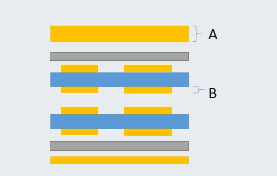
Furthermore, the number of layers in your PCB design can influence the overall thickness.
Multilayer PCBs typically range from four to over twenty layers, with each additional layer contributing to the total thickness. The layer count should be determined based on the complexity of your circuit and the need for signal routing, power distribution, and ground planes. Balancing the layer count with the desired thickness is essential to achieve a functional and manufacturable design.
In conclusion, selecting the right multilayer PCB thickness for your project involves a comprehensive evaluation of electrical performance, mechanical strength, thermal management, and manufacturing constraints. By carefully considering these factors and consulting with your PCB manufacturer, you can make an informed decision that meets the specific needs of your application. This approach will not only enhance the performance and reliability of your electronic device but also ensure a smooth and cost-effective manufacturing process.
The Impact Of Multilayer PCB Thickness On Signal Integrity And Performance
The impact of multilayer PCB thickness on signal integrity and performance is a critical consideration in the design and manufacturing of printed circuit boards (PCBs). As electronic devices become increasingly complex and compact, the demand for multilayer PCBs has surged, necessitating a deeper understanding of how their thickness influences overall functionality.
Multilayer PCBs, which consist of multiple layers of conductive material separated by insulating layers, offer numerous advantages, including enhanced electrical performance, reduced electromagnetic interference (EMI), and greater design flexibility. However, the thickness of these layers plays a pivotal role in determining the signal integrity and performance of the final product.
One of the primary factors affected by multilayer PCB thickness is signal integrity.
Signal integrity refers to the quality and reliability of electrical signals as they travel through the PCB. Thicker PCBs can introduce signal degradation due to increased propagation delay and signal attenuation. Propagation delay, the time it takes for a signal to travel from one point to another, is influenced by the dielectric constant of the insulating material and the physical length of the signal path. In thicker PCBs, the signal path lengthens, leading to greater propagation delay and potential timing issues in high-speed circuits. Additionally, signal attenuation, the reduction in signal strength as it travels through the PCB, can be exacerbated by increased thickness, particularly in high-frequency applications where skin effect and dielectric losses become more pronounced.
Moreover, the thickness of a multilayer PCB can significantly impact its impedance characteristics.
Impedance, the measure of opposition that a circuit presents to the flow of alternating current, is crucial for maintaining signal integrity, especially in high-speed digital and RF circuits. Controlled impedance is often required to ensure that signals are transmitted without reflection or distortion. Thicker PCBs can complicate impedance control due to variations in the dielectric thickness and the potential for increased crosstalk between adjacent signal layers. Crosstalk, the unwanted coupling of signals between nearby traces, can lead to signal interference and degradation, further compromising the performance of the PCB.
Thermal management is another aspect influenced by multilayer PCB thickness.
As electronic components become more powerful and densely packed, effective heat dissipation is essential to prevent overheating and ensure reliable operation. Thicker PCBs can pose challenges in thermal management due to their reduced thermal conductivity. The insulating layers in a multilayer PCB can act as thermal barriers, impeding the efficient transfer of heat away from critical components. This can result in localized hotspots and increased thermal stress, potentially leading to premature failure of the PCB and its components.
Furthermore, the mechanical properties of a multilayer PCB are also affected by its thickness.
Thicker PCBs tend to be more rigid, which can be advantageous in certain applications where mechanical stability is paramount. However, increased rigidity can also make the PCB more susceptible to mechanical stress and potential damage during manufacturing, assembly, and operation. Thinner PCBs, while more flexible, may be prone to warping and bending, which can affect the alignment and connectivity of components.
In conclusion, the thickness of a multilayer PCB has a profound impact on signal integrity and performance. Designers must carefully consider the trade-offs associated with different thicknesses to optimize the electrical, thermal, and mechanical properties of the PCB. By understanding the intricate relationship between PCB thickness and these critical factors, engineers can make informed decisions that enhance the reliability and efficiency of their electronic designs.
Innovations In Multilayer PCB Thickness: Trends And Future Directions
Multilayer printed circuit boards (PCBs) have become indispensable in modern electronics, serving as the backbone for a myriad of devices ranging from smartphones to sophisticated aerospace systems. As technology continues to evolve, the demand for more compact, efficient, and high-performance electronic devices has driven significant innovations in multilayer PCB thickness. These advancements are not only enhancing the functionality of electronic devices but also paving the way for future technological breakthroughs.
One of the primary trends in multilayer PCB thickness is the push towards miniaturization.
As electronic devices become smaller and more powerful, the need for thinner PCBs has become paramount. This trend is particularly evident in consumer electronics, where the demand for sleek, lightweight devices is ever-increasing. To achieve this, manufacturers are employing advanced materials and fabrication techniques that allow for the production of thinner yet robust PCBs. For instance, the use of high-density interconnect (HDI) technology enables the creation of PCBs with finer lines and spaces, thereby reducing the overall thickness without compromising performance.
In addition to miniaturization, there is a growing emphasis on improving the thermal management capabilities of multilayer PCBs.
As electronic components become more densely packed, the heat generated during operation can pose significant challenges. Innovations in PCB materials, such as the incorporation of thermally conductive substrates and advanced copper foils, are helping to address these issues. These materials not only enhance heat dissipation but also contribute to the overall reduction in PCB thickness by eliminating the need for additional cooling mechanisms.
Moreover, the advent of flexible and rigid-flex PCBs is revolutionizing the approach to multilayer PCB thickness.
Flexible PCBs, made from materials like polyimide, offer the advantage of being bendable and foldable, which is particularly beneficial in applications where space constraints are critical. Rigid-flex PCBs combine the best of both worlds, providing the mechanical stability of rigid boards with the adaptability of flexible circuits. These innovations are enabling the design of more compact and versatile electronic devices, further driving the trend towards thinner multilayer PCBs.
Another significant development in this field is the use of advanced manufacturing techniques such as laser drilling and sequential lamination.
Laser drilling allows for the creation of microvias, which are essential for high-density interconnects and contribute to the reduction of PCB thickness. Sequential lamination, on the other hand, involves the layering of multiple thin substrates, which are then bonded together to form a single multilayer PCB. This technique not only ensures precise control over the thickness but also enhances the reliability and performance of the final product.
Looking ahead, the future of multilayer PCB thickness is likely to be shaped by ongoing research and development in materials science and manufacturing technologies. The exploration of novel materials, such as graphene and other nanomaterials, holds promise for further reducing PCB thickness while enhancing electrical and thermal properties. Additionally, advancements in additive manufacturing, or 3D printing, are poised to revolutionize PCB fabrication by enabling the creation of complex, multi-layered structures with unprecedented precision and efficiency.
In conclusion, the innovations in multilayer PCB thickness are driven by the relentless pursuit of miniaturization, improved thermal management, and advanced manufacturing techniques. These trends are not only meeting the current demands of the electronics industry but also setting the stage for future technological advancements. As research and development continue to push the boundaries of what is possible, the future of multilayer PCBs promises to be thinner, more efficient, and more versatile than ever before.