Rf pcb ground plane
Importance Of Rf pcb ground plane
In the realm of RF PCB design, the ground plane holds a position of paramount importance. It serves as the foundation upon which the entire circuit’s performance is built.
The ground plane, essentially a large area of copper on the PCB, acts as a reference point for all signals and provides a return path for current. Its significance cannot be overstated, as it directly influences the integrity and efficiency of the RF signals.
One of the primary reasons the ground plane is crucial in RF PCB design is its role in minimizing electromagnetic interference (EMI).
EMI can severely degrade the performance of RF circuits, leading to signal loss and increased noise. By providing a continuous and low-impedance path for return currents, the ground plane helps to shield sensitive components from external noise sources. This shielding effect is particularly vital in high-frequency applications where even minor disruptions can have substantial impacts.
Moreover, the ground plane contributes to the reduction of signal crosstalk.
Crosstalk occurs when signals from adjacent traces interfere with each other, causing unwanted noise and potential data corruption. A well-designed ground plane ensures that the return currents flow directly beneath their corresponding signal traces, thereby minimizing the loop area and reducing the likelihood of crosstalk. This is especially important in densely packed PCBs where space constraints make it challenging to maintain adequate separation between traces.
In addition to mitigating EMI and crosstalk, the ground plane plays a critical role in maintaining signal integrity.
High-frequency signals are particularly susceptible to reflections and impedance mismatches, which can distort the signal and degrade performance. The ground plane helps to maintain a consistent impedance along the signal path, thereby reducing reflections and ensuring that the signal reaches its destination with minimal distortion. This is achieved by providing a uniform reference plane that helps to control the characteristic impedance of the transmission lines.
Furthermore, the ground plane aids in thermal management, which is an often-overlooked aspect of RF PCB design.
High-frequency components can generate significant amounts of heat, which, if not properly managed, can lead to thermal stress and potential failure. The ground plane acts as a heat sink, dissipating heat away from critical components and helping to maintain a stable operating temperature. This not only enhances the reliability of the circuit but also extends the lifespan of the components.
Another important consideration is the role of the ground plane in power distribution. In RF circuits, maintaining a stable and noise-free power supply is essential for optimal performance. The ground plane helps to distribute power evenly across the PCB, reducing voltage drops and ensuring that all components receive a consistent supply of power. This is particularly important in RF applications where even minor fluctuations in power can lead to significant performance degradation.
In conclusion, the ground plane is an indispensable element in RF PCB design. Its ability to minimize EMI, reduce crosstalk, maintain signal integrity, aid in thermal management, and ensure stable power distribution underscores its critical role in the overall performance of RF circuits. As such, careful consideration and meticulous design of the ground plane are essential for achieving optimal results in RF PCB applications. By understanding and leveraging the benefits of a well-designed ground plane, engineers can significantly enhance the performance and reliability of their RF circuits.

Techniques For Optimizing Ground Plane In RF PCBs
In the realm of radio frequency (RF) printed circuit boards (PCBs), the ground plane plays a pivotal role in ensuring optimal performance and signal integrity. As RF circuits operate at high frequencies, any imperfections in the ground plane can lead to significant issues such as signal loss, noise, and electromagnetic interference (EMI). Therefore, optimizing the ground plane in RF PCBs is crucial for achieving reliable and efficient designs. Several techniques can be employed to enhance the ground plane, each contributing to the overall performance of the RF PCB.
One fundamental technique is to ensure that the ground plane is as continuous and unbroken as possible.
Interruptions in By incorporating several ground layers, designers can reduce the overall impedance of the ground plane, which is particularly beneficial for high-frequency applications. These multiple ground layers can be connected through vias, creating a low-impedance path for return currents and further enhancing signal integrity. Moreover, the use of multiple ground layers can help in distributing heat more evenly across the PCB, thereby improving thermal management.
The placement of vias is another crucial consideration when optimizing the ground plane in RF PCBs.
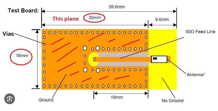
Vias are used to connect different layers of the PCB, and their placement can significantly impact the performance of the ground plane. It is advisable to place vias strategically to ensure a low-impedance path for return currents. For instance, placing vias close to signal traces can help in minimizing the loop area, thereby reducing inductance and improving signal integrity. Additionally, using a sufficient number of vias can help in maintaining a continuous ground plane across different layers of the PCB.
Furthermore, the use of ground pours and stitching vias can be highly effective in optimizing the ground plane.
Ground pours are large areas of copper connected to the ground plane, which can help in reducing EMI and providing a stable reference for RF signals. Stitching vias, on the other hand, are used to connect ground pours on different layers, creating a more robust and continuous ground plane. By strategically placing ground pours and stitching vias, designers can enhance the overall performance of the RF PCB.
In addition to these techniques, careful consideration of the PCB layout is essential for optimizing the ground plane.
The layout should be designed to minimize the length of signal traces and ensure that return paths are as short and direct as possible. This can help in reducing the loop area and minimizing inductance, thereby improving signal integrity. Moreover, it is important to keep high-frequency components and sensitive analog circuits away from noisy digital circuits to prevent interference.
In conclusion, optimizing the ground plane in RF PCBs is a multifaceted process that involves several techniques, each contributing to the overall performance and reliability of the design. By ensuring a continuous and unbroken ground plane, using multiple ground layers, strategically placing vias, incorporating ground pours and stitching vias, and carefully designing the PCB layout, designers can achieve optimal performance in their RF PCB designs. These techniques, when applied effectively, can help in minimizing signal loss, reducing EMI, and ensuring the integrity of high-frequency signals, ultimately leading to more efficient and reliable RF circuits.

Common Mistakes In RF PCB Ground Plane Design
Designing the ground plane for an RF PCB is a critical task that can significantly impact the performance of the final product. However, it is not uncommon for designers to make mistakes that can lead to suboptimal performance or even complete failure of the RF system.
One of the most frequent errors is neglecting the importance of a continuous ground plane.
A fragmented or discontinuous ground plane can introduce unwanted inductance and resistance, which can degrade signal integrity and increase electromagnetic interference (EMI). Therefore, ensuring a solid, unbroken ground plane is essential for maintaining the integrity of the RF signals.
Another common mistake is improper placement of vias.
Vias are used to connect different layers of a PCB, and their placement can significantly affect the performance of the ground plane. Placing vias too far apart can create impedance discontinuities, which can lead to signal reflections and loss. On the other hand, placing them too close together can result in excessive parasitic capacitance. Therefore, it is crucial to carefully plan the placement of vias to balance these factors and maintain a low-impedance path for the return currents.
In addition to via placement, the location of components on the PCB can also impact the effectiveness of the ground plane.
Placing components too close to the edge of the PCB can cause the ground plane to be less effective in shielding the RF signals from external noise. This is because the edge of the PCB is more susceptible to EMI. To mitigate this, it is advisable to place critical RF components away from the edges and closer to the center of the PCB, where the ground plane can provide better shielding.
Furthermore, designers often overlook the importance of proper grounding techniques.
For instance, using a single-point ground can be beneficial in some low-frequency applications, but it is generally not suitable for RF designs. A single-point ground can create ground loops, which can introduce noise and degrade signal quality. Instead, a multi-point ground or a ground grid is usually more effective in RF designs, as it provides multiple low-impedance paths for the return currents, thereby reducing the risk of ground loops.
Another pitfall is the improper handling of power and ground planes.
In some cases, designers may be tempted to combine power and ground planes to save space or reduce costs. However, this can lead to significant performance issues, as the power plane can introduce noise into the ground plane, thereby degrading the performance of the RF signals. It is generally advisable to keep power and ground planes separate and to use decoupling capacitors to filter out any noise that may be present on the power plane.
Lastly, thermal management is another aspect that is often neglected in RF PCB ground plane design.
High-frequency signals can generate significant amounts of heat, which can affect the performance and reliability of the PCB. Therefore, it is important to consider thermal management techniques, such as using thermal vias and heat sinks, to dissipate the heat generated by the RF components.
In conclusion, designing an effective RF PCB ground plane requires careful consideration of various factors, including the continuity of the ground plane, via placement, component location, grounding techniques, separation of power and ground planes, and thermal management. By avoiding these common mistakes, designers can ensure that their RF PCBs perform optimally and reliably.

Impact Of Ground Plane On Signal Integrity In RF PCBs
In the realm of radio frequency (RF) printed circuit boards (PCBs), the ground plane plays a pivotal role in maintaining signal integrity. As RF circuits operate at high frequencies, even minor disruptions can lead to significant performance degradation. Therefore, understanding the impact of the ground plane on signal integrity is crucial for engineers and designers working with RF PCBs.
To begin with, the ground plane serves as a reference point for all signals on the PCB.
It provides a low-impedance path for return currents, which is essential for minimizing noise and ensuring stable signal transmission. When the ground plane is well-designed, it helps to reduce electromagnetic interference (EMI) and crosstalk between adjacent traces. This is particularly important in RF applications, where signals are highly susceptible to external noise and interference.
Moreover, the ground plane’s effectiveness is influenced by its layout and placement.
A continuous and unbroken ground plane is ideal, as it offers a consistent reference point for all signals. Interruptions in the ground plane, such as gaps or splits, can cause impedance discontinuities, leading to signal reflections and potential data loss. Therefore, designers must carefully plan the ground plane layout to avoid such disruptions and ensure a smooth signal path.
In addition to layout considerations, the proximity of the ground plane to signal traces also impacts signal integrity.
Placing the ground plane close to the signal layer helps to create a controlled impedance environment, which is essential for high-frequency signal transmission. This proximity reduces the loop area for return currents, thereby minimizing inductive coupling and potential EMI issues. Consequently, maintaining a close distance between the ground plane and signal traces is a best practice in RF PCB design.
Furthermore, the ground plane’s role extends to thermal management.
High-frequency signals generate heat, which can affect the performance and reliability of the PCB. The ground plane acts as a heat sink, dissipating heat away from critical components and preventing thermal buildup. This thermal management capability is particularly important in RF applications, where maintaining stable operating temperatures is crucial for optimal performance.
Another aspect to consider is the use of multiple ground planes in multilayer PCBs.
In complex RF designs, multiple ground planes can provide additional benefits, such as improved signal isolation and reduced EMI. By strategically placing ground planes between signal layers, designers can create effective shielding and minimize interference. However, it is essential to ensure proper grounding and via placement to maintain connectivity between the ground planes and avoid potential issues.
Transitioning to the topic of grounding techniques, it is important to highlight the significance of proper grounding in RF PCB design.
Grounding techniques, such as star grounding and ground stitching, help to establish a solid ground reference and minimize ground loops. These techniques ensure that all components have a common ground potential, reducing the risk of noise and interference. Implementing effective grounding techniques is a key factor in achieving high signal integrity in RF PCBs.
In conclusion, the ground plane is a critical element in RF PCB design, significantly impacting signal integrity. A well-designed ground plane provides a stable reference point, minimizes noise and interference, and aids in thermal management. By carefully considering the layout, proximity to signal traces, and grounding techniques, designers can optimize the ground plane’s effectiveness and ensure reliable performance in RF applications. As RF technology continues to advance, the importance of a robust ground plane in maintaining signal integrity cannot be overstated.
