Rf pcb ground vias
Importance Of Rf pcb ground vias
In the realm of Radio Frequency (RF) Printed Circuit Board (PCB) design, the importance of ground vias cannot be overstated. Ground vias serve as critical components that ensure the integrity and performance of RF circuits.
These small, yet significant, elements facilitate the connection between different layers of a PCB, providing a low-impedance path to the ground plane. This is particularly crucial in RF applications where signal integrity and electromagnetic compatibility (EMC) are paramount.
To begin with, ground vias play a pivotal role in minimizing the inductance and resistance in the ground path.
In RF circuits, high-frequency signals are highly susceptible to noise and interference. Any inductance in the ground path can lead to unwanted voltage drops, which can degrade the performance of the circuit. By providing a direct and low-impedance connection to the ground plane, ground vias help in maintaining a stable reference potential across the PCB. This, in turn, ensures that the signal integrity is preserved, and the circuit operates as intended.
Moreover, ground vias are essential for effective electromagnetic shielding.
In RF PCB design, it is common to encounter issues related to electromagnetic interference (EMI). Ground vias help in creating a Faraday cage effect by connecting the ground planes on different layers of the PCB. This shielding effect is crucial for preventing external electromagnetic fields from interfering with the sensitive RF signals. Additionally, it helps in containing the electromagnetic emissions from the circuit itself, thereby ensuring compliance with regulatory standards for EMC.
Another significant aspect of ground vias is their role in thermal management.
RF circuits often generate substantial amounts of heat, which needs to be dissipated efficiently to prevent damage to the components. Ground vias facilitate the transfer of heat from the surface-mounted components to the inner layers of the PCB, where it can be spread out and dissipated more effectively. This thermal conduction pathway is vital for maintaining the reliability and longevity of the RF circuit.
Furthermore, the placement and number of ground vias are critical factors that influence the overall performance of the RF PCB.
Strategic placement of ground vias can help in reducing the loop area of the return current path, thereby minimizing the potential for radiated emissions. It is generally recommended to place ground vias as close as possible to the signal vias to ensure a short and direct return path. Additionally, using an adequate number of ground vias can help in distributing the current evenly across the ground plane, which is essential for maintaining a low-impedance ground reference.
In addition to their functional benefits, ground vias also contribute to the mechanical stability of the PCB.
They provide additional points of connection between the layers, which can enhance the structural integrity of the board. This is particularly important in applications where the PCB may be subjected to mechanical stress or vibration.
In conclusion, ground vias are indispensable elements in RF PCB design, offering a multitude of benefits that are crucial for the optimal performance of RF circuits. They ensure low-impedance ground connections, provide effective electromagnetic shielding, aid in thermal management, and enhance mechanical stability. By carefully considering the placement and number of ground vias, designers can significantly improve the signal integrity, EMC performance, and overall reliability of RF PCBs. As such, ground vias should be given due attention and consideration in the design process to achieve the best possible outcomes in RF applications.
Best Practices For Placing Ground Vias In RF PCBs
When designing RF printed circuit boards (PCBs), the placement of ground vias is a critical factor that significantly influences the performance and reliability of the circuit. Ground vias serve as electrical connections between different layers of the PCB, providing a low-impedance path to the ground plane. Proper placement of these vias is essential to minimize electromagnetic interference (EMI), reduce signal loss, and ensure signal integrity. To achieve optimal performance, several best practices should be followed when placing ground vias in RF PCBs.
Firstly, it is important to understand the role of ground vias in maintaining signal integrity.
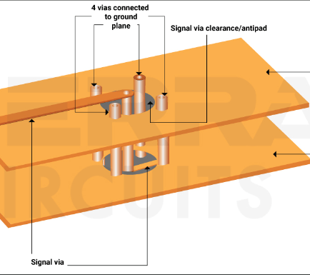
In RF circuits, signals travel at high frequencies, and any impedance mismatch can lead to signal reflections and losses. Ground vias help to create a continuous ground plane, which is crucial for maintaining a consistent impedance along the signal path. By strategically placing ground vias near signal traces, designers can ensure that the return current flows through the shortest possible path, thereby minimizing inductive loops and reducing EMI.
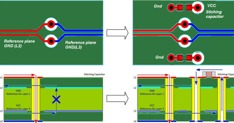
One of the best practices for placing ground vias is to use a via stitching technique.
Via stitching involves placing multiple ground vias around the perimeter of the signal traces and components. This technique helps to create a solid ground plane, which is essential for shielding the signal traces from external noise and preventing crosstalk between adjacent traces. Additionally, via stitching can help to reduce the loop area of the return current, thereby minimizing the inductive effects and improving the overall performance of the RF circuit.
Another important consideration is the spacing between ground vias.
The spacing should be small enough to ensure a continuous ground plane but not so small that it compromises the mechanical integrity of the PCB. A common rule of thumb is to place ground vias at intervals of one-tenth of the wavelength of the highest frequency signal in the circuit. This spacing ensures that the ground plane remains effective at high frequencies, providing a low-impedance path for the return current.
Furthermore, it is essential to place ground vias near critical components and signal transitions.
For example, ground vias should be placed near connectors, where signals enter or exit the PCB, to provide a low-impedance path for the return current. Similarly, ground vias should be placed near any discontinuities in the signal path, such as bends or vias, to minimize impedance mismatches and signal reflections. By placing ground vias strategically, designers can ensure that the return current flows through the shortest possible path, thereby reducing signal loss and improving the overall performance of the RF circuit.
In addition to these considerations, it is also important to use multiple ground vias for high-current paths.
High-current paths, such as power supply lines, can generate significant EMI if not properly grounded. By using multiple ground vias, designers can ensure that the return current is evenly distributed across the ground plane, thereby reducing EMI and improving the overall performance of the RF circuit.
Finally, it is important to consider the thermal management of the PCB when placing ground vias.
Ground vias can help to dissipate heat generated by high-power components, thereby improving the reliability and longevity of the PCB. By placing ground vias near high-power components, designers can ensure that heat is efficiently transferred to the ground plane, thereby reducing the risk of thermal damage and improving the overall performance of the RF circuit.
In conclusion, the placement of ground vias is a critical factor in the design of RF PCBs. By following best practices such as via stitching, optimizing via spacing, strategically placing ground vias near critical components and signal transitions, using multiple ground vias for high-current paths, and considering thermal management, designers can ensure that their RF circuits achieve optimal performance and reliability.
Common Mistakes To Avoid With RF PCB Ground Vias
When designing RF PCBs, ground vias play a crucial role in ensuring signal integrity and minimizing electromagnetic interference. However, several common mistakes can compromise the performance of these circuits.
One frequent error is the improper placement of ground vias.
Placing them too far from the signal path can lead to increased inductance, which in turn can degrade signal quality. To mitigate this, it is essential to position ground vias as close to the signal traces as possible, thereby reducing the loop area and minimizing inductive effects.
Another prevalent mistake is the insufficient number of ground vias.
A sparse distribution of ground vias can result in poor grounding, leading to increased noise and potential signal integrity issues. To avoid this, designers should ensure an adequate number of ground vias are used, particularly around critical components and high-frequency signal paths. This helps to create a low-impedance path to ground, which is vital for maintaining signal integrity.
Moreover, the size and type of ground vias can also impact performance.
Using vias that are too small can increase their inductance, which can be detrimental at high frequencies. Conversely, using vias that are too large can take up excessive space on the PCB, potentially interfering with other components and traces. Therefore, it is important to select the appropriate via size based on the specific requirements of the design. Additionally, using blind or buried vias can help to save space and reduce parasitic effects, although these options may increase manufacturing complexity and cost.
Thermal management is another critical aspect that can be overlooked.
Ground vias not only provide electrical connectivity but also play a role in heat dissipation. Failing to account for thermal considerations can lead to overheating and potential damage to the PCB and its components. To address this, designers should ensure that ground vias are adequately distributed to facilitate effective heat dissipation. This is particularly important in high-power applications where thermal management is a key concern.
Furthermore, the quality of the via plating is often underestimated.
Poorly plated vias can result in increased resistance and potential reliability issues over time. Ensuring high-quality via plating is essential for maintaining low resistance and ensuring long-term reliability. This can be achieved by working with reputable PCB manufacturers and specifying stringent quality control measures.
In addition to these technical considerations, it is also important to be mindful of the overall design process.
Inadequate simulation and testing can lead to unforeseen issues that may not be apparent during the initial design phase. Utilizing advanced simulation tools and conducting thorough testing can help to identify and address potential problems before they become critical. This proactive approach can save time and resources in the long run, ensuring a more robust and reliable design.
Lastly, communication and collaboration with the manufacturing team are vital.
Designers should work closely with manufacturers to ensure that the design is feasible and can be produced to the required specifications. This collaborative approach can help to identify potential issues early in the process and ensure a smoother transition from design to production.
In conclusion, avoiding common mistakes with RF PCB ground vias requires careful consideration of placement, quantity, size, thermal management, via plating quality, and thorough testing. By addressing these factors and fostering effective communication with manufacturers, designers can enhance the performance and reliability of their RF PCBs, ultimately leading to more successful and efficient designs.
Impact Of Ground Vias On RF Signal Integrity
In the realm of radio frequency (RF) circuit design, the integrity of the signal is paramount. One critical aspect that significantly influences RF signal integrity is the implementation of ground vias on printed circuit boards (PCBs). Ground vias, which are conductive pathways that connect different layers of a PCB, play a crucial role in maintaining the performance and reliability of RF circuits. Their impact on signal integrity cannot be overstated, as they contribute to minimizing noise, reducing electromagnetic interference (EMI), and ensuring proper grounding.
To begin with, ground vias are essential for providing a low-impedance path to the ground plane.
This is particularly important in RF circuits, where high-frequency signals are susceptible to noise and interference. By offering a direct route to the ground plane, ground vias help to stabilize the voltage levels and reduce the potential for signal distortion. This stabilization is crucial for maintaining the fidelity of the RF signal, as any deviation can lead to performance degradation and communication errors.
Moreover, ground vias play a pivotal role in mitigating electromagnetic interference.
EMI is a common challenge in RF circuit design, as high-frequency signals can easily couple with adjacent traces and components, leading to unwanted noise and signal degradation. Ground vias help to confine the return currents to the ground plane, thereby minimizing the loop area and reducing the potential for EMI. This containment is vital for ensuring that the RF signal remains clean and free from external disturbances, which is essential for achieving optimal performance.
In addition to reducing EMI, ground vias also contribute to the overall thermal management of the PCB.
High-frequency RF circuits often generate significant amounts of heat, which can adversely affect the performance and longevity of the components. Ground vias facilitate the dissipation of heat by providing a thermal pathway to the ground plane, thereby helping to maintain the temperature within acceptable limits. This thermal management is crucial for preventing overheating and ensuring the reliable operation of the RF circuit.
Furthermore, the placement and density of ground vias are critical factors that influence their effectiveness.
Strategically placing ground vias near critical components and along the signal path can significantly enhance the grounding and shielding capabilities of the PCB. A higher density of ground vias can provide a more robust grounding network, which is particularly beneficial in high-frequency applications. However, it is essential to strike a balance, as an excessive number of ground vias can lead to increased parasitic capacitance and inductance, which can negatively impact the signal integrity.
It is also worth noting that the design and implementation of ground vias require careful consideration of the PCB stack-up and layer configuration. The choice of materials, the thickness of the layers, and the spacing between the vias all play a role in determining the overall performance of the RF circuit. Properly designed ground vias can enhance the signal integrity by providing a consistent and reliable grounding path, while poorly designed vias can introduce unwanted impedance and signal reflections.
In conclusion, ground vias are a fundamental component in RF PCB design, with a significant impact on signal integrity. By providing a low-impedance path to the ground plane, mitigating electromagnetic interference, aiding in thermal management, and ensuring proper grounding, ground vias contribute to the overall performance and reliability of RF circuits. Careful consideration of their placement, density, and design is essential for achieving optimal signal integrity and ensuring the successful operation of RF systems.