Rf pcb layout techniques
Best Practices For Rf pcb layout techniques
Designing a printed circuit board (PCB) for radio frequency (RF) applications requires meticulous attention to detail and adherence to best practices to ensure optimal performance. The complexity of RF signals, which are highly sensitive to layout variations, necessitates a strategic approach to PCB design.
One of the fundamental principles in RF PCB layout is maintaining signal integrity.
This can be achieved by minimizing signal path lengths and avoiding sharp bends, which can cause signal reflections and losses. Utilizing microstrip or stripline configurations for transmission lines helps in controlling impedance and reducing signal degradation.
Another critical aspect is the careful management of grounding.
A solid ground plane is essential for providing a low-impedance return path for RF signals, thereby minimizing noise and interference. Ensuring that the ground plane is continuous and free of gaps is crucial, as any discontinuities can lead to unwanted resonances and signal integrity issues. Additionally, the use of via stitching around the perimeter of the ground plane can further enhance its effectiveness by reducing the potential for ground loops.
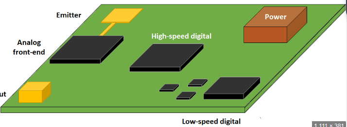
Component placement also plays a significant role in RF PCB layout.
Placing components in close proximity to each other can reduce parasitic inductance and capacitance, which are detrimental to RF performance. It is advisable to place sensitive components, such as oscillators and amplifiers, away from noisy digital circuits to prevent electromagnetic interference (EMI). Furthermore, aligning components along the same axis as the signal flow can help in maintaining signal integrity and reducing crosstalk.
The choice of materials is another important consideration.
High-frequency laminates, such as Rogers or Taconic, offer superior dielectric properties compared to standard FR4 materials, resulting in lower signal loss and better performance at high frequencies. These materials also exhibit more stable dielectric constants, which is crucial for maintaining consistent impedance throughout the PCB.
Thermal management is equally important in RF PCB design.
High-power RF components can generate significant heat, which, if not properly managed, can lead to performance degradation or even component failure. Incorporating thermal vias and heat sinks can help in dissipating heat effectively. Additionally, ensuring adequate spacing between components can facilitate better airflow and heat dissipation.
Shielding is another technique that can be employed to protect sensitive RF circuits from external EMI.
Using metal enclosures or shielding cans can effectively isolate RF components from external noise sources. However, it is important to ensure that the shielding does not interfere with the signal paths or create unwanted resonances.
Simulation and testing are indispensable steps in the RF PCB design process.
Using simulation tools to model the PCB layout can help in identifying potential issues before the physical prototype is built. Post-layout simulation can provide insights into signal integrity, impedance matching, and EMI performance. Once the PCB is fabricated, thorough testing using network analyzers and spectrum analyzers is essential to verify that the design meets the required specifications.
In conclusion, designing an RF PCB requires a comprehensive understanding of RF principles and meticulous attention to detail.
By adhering to best practices such as maintaining signal integrity, managing grounding effectively, optimizing component placement, selecting appropriate materials, managing thermal performance, and employing shielding techniques, designers can achieve high-performance RF PCBs. Simulation and testing further ensure that the final product meets the desired performance criteria, thereby enabling reliable and efficient RF applications.
Minimizing Signal Interference In RF PCB Layouts
Minimizing signal interference in RF PCB layouts is a critical aspect of ensuring optimal performance in radio frequency circuits. Signal interference can significantly degrade the functionality of RF systems, leading to issues such as signal loss, noise, and crosstalk. Therefore, employing effective RF PCB layout techniques is essential to mitigate these problems and achieve reliable operation.
One of the primary considerations in minimizing signal interference is the careful management of signal paths.
Ensuring that signal traces are as short and direct as possible can reduce the potential for interference. Long traces can act as antennas, picking up unwanted signals and radiating noise. By keeping traces short, the likelihood of such issues is minimized. Additionally, maintaining a consistent trace width is crucial, as variations can lead to impedance mismatches, which in turn can cause signal reflections and interference.
Another important technique involves the strategic placement of components.
Placing sensitive components, such as low-noise amplifiers and oscillators, away from high-power or noisy components can help reduce interference. Grouping components with similar functions together and separating them from other groups can also aid in minimizing crosstalk. Furthermore, placing decoupling capacitors close to the power pins of active components can help filter out high-frequency noise, thereby reducing interference.
Grounding is another critical aspect of RF PCB layout.
A solid ground plane can provide a low-impedance path for return currents, which helps in minimizing noise and interference. Ensuring that the ground plane is continuous and unbroken is essential, as gaps or splits can create potential points of interference. Additionally, using multiple ground vias to connect the ground plane to different layers of the PCB can further enhance grounding effectiveness.
Shielding is also an effective method for minimizing signal interference.
Enclosing sensitive components or entire sections of the PCB in metal shields can prevent external noise from affecting the circuit. Shielding can also contain any noise generated within the circuit, preventing it from radiating and causing interference with other parts of the system. However, it is important to ensure that the shields are properly grounded to avoid creating additional interference.
The use of differential signaling can also help in reducing interference.
Differential pairs, which consist of two traces carrying equal and opposite signals, can cancel out common-mode noise. This technique is particularly useful in high-speed and high-frequency applications, where signal integrity is paramount. Ensuring that differential pairs are routed closely together and have matched lengths is crucial for maintaining their effectiveness.
Moreover, careful consideration of the PCB stack-up can play a significant role in minimizing signal interference.
A well-designed stack-up can provide controlled impedance for signal traces, reducing the potential for reflections and crosstalk. Placing signal layers adjacent to ground or power planes can also help in shielding signals from interference.
In conclusion, minimizing signal interference in RF PCB layouts requires a comprehensive approach that includes managing signal paths, strategic component placement, effective grounding, shielding, differential signaling, and careful stack-up design. By employing these techniques, designers can significantly enhance the performance and reliability of RF circuits, ensuring that they operate effectively in their intended applications.
Importance Of Ground Planes In RF PCB Layouts
In the realm of RF PCB (Radio Frequency Printed Circuit Board) design, the importance of ground planes cannot be overstated. Ground planes serve as a critical component in ensuring the optimal performance of RF circuits, which are inherently sensitive to noise and interference. By providing a low-impedance path to ground, ground planes help to minimize electromagnetic interference (EMI) and signal crosstalk, thereby enhancing the overall integrity of the RF signals.
One of the primary functions of a ground plane is to act as a reference point for all signals within the circuit.
This reference point is essential for maintaining signal integrity, as it ensures that all components within the RF PCB have a common ground potential. Without a consistent ground reference, signal levels can fluctuate, leading to erratic behavior and potential malfunction of the circuit. Moreover, ground planes help to reduce the loop area of signal paths, which in turn minimizes the inductance and susceptibility to external noise sources.
In addition to providing a stable reference point, ground planes also play a crucial role in shielding sensitive RF components from external electromagnetic fields.
By creating a continuous conductive layer beneath the signal traces, ground planes effectively block unwanted EMI from penetrating the circuit. This shielding effect is particularly important in high-frequency applications, where even minor interference can significantly degrade signal quality. Furthermore, ground planes can help to confine the electromagnetic fields generated by the RF signals themselves, preventing them from radiating and causing interference with other nearby circuits.
Another key advantage of ground planes in RF PCB layouts is their ability to facilitate efficient heat dissipation.
RF components, such as power amplifiers and oscillators, often generate significant amounts of heat during operation. A well-designed ground plane can act as a heat sink, spreading the thermal energy across a larger area and preventing localized hotspots that could damage the components. This thermal management capability is essential for maintaining the reliability and longevity of the RF circuit.
Moreover, ground planes contribute to the overall mechanical stability of the PCB.
By providing a solid, continuous layer of copper, ground planes enhance the structural integrity of the board, reducing the risk of warping or bending. This mechanical stability is particularly important in applications where the PCB may be subjected to physical stress or vibration.
To maximize the benefits of ground planes in RF PCB layouts, it is essential to follow best practices during the design process.
For instance, designers should strive to maintain a continuous ground plane with minimal interruptions. Any gaps or discontinuities in the ground plane can create impedance mismatches and potential points of EMI ingress. Additionally, it is advisable to place ground vias strategically to ensure a low-impedance connection between different layers of the PCB. These vias help to maintain a consistent ground potential across the entire board, further enhancing signal integrity.
In conclusion, ground planes are an indispensable element in RF PCB layouts, offering numerous benefits that contribute to the optimal performance of RF circuits. By providing a stable reference point, shielding against EMI, facilitating heat dissipation, and enhancing mechanical stability, ground planes play a pivotal role in ensuring the reliability and efficiency of RF designs. Adhering to best practices in ground plane implementation is essential for achieving the desired performance and minimizing potential issues in RF PCB layouts.

Techniques For Impedance Matching In RF PCB Design
Impedance matching is a critical aspect of RF PCB design, ensuring that the maximum amount of power is transferred from the source to the load with minimal reflection and loss. Achieving effective impedance matching requires a thorough understanding of various techniques and principles. One fundamental technique involves the use of transmission lines, which are designed to have a characteristic impedance that matches the source and load impedances. This can be accomplished by carefully selecting the width and spacing of the traces on the PCB, as well as the dielectric material used.
Another essential technique is the use of matching networks, which can be implemented using discrete components such as inductors and capacitors.
These components are arranged in specific configurations, such as L-networks, T-networks, or Pi-networks, to transform the impedance of the source to match that of the load. The choice of network topology depends on the specific impedance values and the frequency range of the RF signal. Additionally, the quality factor (Q) of the components must be considered, as it affects the overall performance and efficiency of the matching network.
Microstrip lines are also commonly used in RF PCB design for impedance matching.
These lines consist of a conducting strip separated from a ground plane by a dielectric layer. By adjusting the width of the microstrip line and the thickness of the dielectric layer, designers can achieve the desired characteristic impedance. Furthermore, the use of coplanar waveguides, which have ground planes on either side of the signal trace, can provide better isolation and reduced crosstalk, thereby improving impedance matching.
Incorporating vias and ground planes is another technique that plays a significant role in impedance matching.
Vias are used to connect different layers of the PCB, and their placement must be carefully considered to minimize inductance and resistance. Ground planes, on the other hand, provide a low-impedance return path for the RF signals, reducing noise and improving signal integrity. Ensuring a continuous and unbroken ground plane beneath the signal traces is crucial for maintaining consistent impedance.
Moreover, the use of simulation tools is indispensable in the design process.
These tools allow designers to model and analyze the impedance characteristics of the PCB layout, enabling them to make necessary adjustments before fabrication. Electromagnetic simulation software can predict the behavior of the RF signals and identify potential issues such as impedance mismatches, signal reflections, and losses. By iterating through simulations, designers can optimize the layout for better impedance matching and overall performance.
Additionally, proper termination techniques are vital for impedance matching.
Termination resistors are used to match the impedance of the transmission line to the load, preventing signal reflections. The value of the termination resistor should be equal to the characteristic impedance of the transmission line. In some cases, active components such as amplifiers or attenuators may be used for impedance matching, especially in complex RF systems where passive components alone are insufficient.
In conclusion, achieving effective impedance matching in RF PCB design requires a combination of techniques, including the use of transmission lines, matching networks, microstrip lines, vias, ground planes, and simulation tools. Each technique must be carefully considered and implemented to ensure optimal performance and signal integrity. By understanding and applying these techniques, designers can create RF PCBs that deliver reliable and efficient performance in a wide range of applications.