What is 4 layer pcb
What is 4 layer pcb
A 4-layer printed circuit board (PCB) is a sophisticated and highly efficient type of PCB that is widely used in various electronic applications. Unlike the more common single-layer or double-layer PCBs, a 4-layer PCB consists of four layers of conductive material, typically copper, separated by insulating layers. This multi-layer structure allows for greater complexity and functionality in electronic circuits, making it an essential component in modern electronics.
To understand the structure of a 4-layer PCB, it is important to first grasp the basic concept of a PCB.
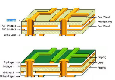
A PCB is a board that mechanically supports and electrically connects electronic components using conductive pathways, or traces, etched from copper sheets laminated onto a non-conductive substrate. In a 4-layer PCB, these conductive pathways are distributed across four distinct layers. The typical configuration includes two outer layers and two inner layers. The outer layers are usually used for signal routing, while the inner layers are often dedicated to power distribution and ground planes.
The construction of a 4-layer PCB begins with a core material, which is a thin, rigid substrate with copper foil laminated on both sides.
This core forms the central part of the PCB. Additional layers of copper and insulating material, known as prepreg, are then added to the core. The entire stack is subjected to heat and pressure to bond the layers together, creating a single, cohesive board. Vias, or small holes drilled through the board, are used to connect the different layers electrically. These vias can be through-hole, blind, or buried, depending on their placement and function.
One of the primary benefits of a 4-layer PCB is its ability to support more complex and higher-density circuits.
The additional layers provide more routing space, allowing designers to create more intricate and compact designs. This is particularly advantageous in applications where space is at a premium, such as in smartphones, tablets, and other portable devices. Moreover, the use of dedicated power and ground planes in the inner layers helps to reduce electromagnetic interference (EMI) and improve signal integrity. This results in more reliable and stable electronic performance.
Another significant advantage of 4-layer PCBs is their enhanced thermal management capabilities.
The multiple layers can dissipate heat more effectively, preventing overheating and ensuring the longevity of the electronic components. This is especially crucial in high-power applications, such as in industrial equipment and automotive electronics, where efficient heat dissipation is essential for maintaining optimal performance.
Furthermore, 4-layer PCBs offer improved electrical performance due to the reduced signal path lengths and lower inductance.
The close proximity of the power and ground planes helps to minimize voltage drops and noise, leading to better overall circuit performance. This makes 4-layer PCBs ideal for high-speed and high-frequency applications, such as in telecommunications and networking equipment.
In conclusion, a 4-layer PCB is a versatile and highly efficient solution for modern electronic designs. Its multi-layer structure provides numerous benefits, including increased circuit complexity, improved thermal management, and enhanced electrical performance. As electronic devices continue to evolve and demand more advanced features, the use of 4-layer PCBs is likely to become even more prevalent, solidifying their role as a cornerstone of contemporary electronics.
Design Considerations For 4 Layer PCB Layout
When designing a 4-layer printed circuit board (PCB), several critical considerations must be taken into account to ensure optimal performance and reliability. A 4-layer PCB typically consists of two outer layers and two inner layers, which are used for routing signals and providing power and ground planes. This configuration offers enhanced electrical performance, reduced electromagnetic interference (EMI), and improved signal integrity compared to simpler, two-layer designs. However, the complexity of a 4-layer PCB necessitates careful planning and attention to detail during the design process.
One of the primary considerations in 4-layer PCB design is the stack-up configuration.
The stack-up refers to the arrangement of the different layers within the PCB. A common stack-up for a 4-layer PCB includes a top signal layer, an inner ground plane, an inner power plane, and a bottom signal layer. This configuration helps to minimize EMI and crosstalk by providing a solid ground plane and power plane that can effectively shield and separate the signal layers. Additionally, the proximity of the power and ground planes helps to reduce the loop inductance, which is crucial for maintaining signal integrity, especially in high-speed digital circuits.
Another important aspect of 4-layer PCB design is the routing of signal traces.
Proper trace routing is essential to avoid issues such as signal reflection, crosstalk, and impedance mismatches. To achieve this, designers should follow best practices such as maintaining consistent trace widths, using controlled impedance traces for high-speed signals, and avoiding sharp bends in the traces. Furthermore, it is advisable to route high-speed signals on the inner layers, where they are shielded by the power and ground planes, thereby reducing the risk of EMI.
The placement of components on a 4-layer PCB also requires careful consideration.
Components should be strategically placed to minimize the length of critical signal paths and to ensure efficient power distribution. Grouping related components together can help to reduce the complexity of the routing and improve the overall performance of the PCB. Additionally, designers should pay attention to the placement of decoupling capacitors, which are used to filter out noise and provide a stable power supply to the components. These capacitors should be placed as close as possible to the power pins of the integrated circuits to maximize their effectiveness.
Thermal management is another crucial factor in 4-layer PCB design.
The increased density of components and traces in a 4-layer PCB can lead to higher levels of heat generation, which can adversely affect the performance and reliability of the board. To address this, designers should incorporate thermal vias, which are small holes that connect the different layers of the PCB and allow heat to dissipate more effectively. Additionally, the use of thermal relief pads can help to improve heat dissipation and prevent overheating of critical components.
Finally, designers must consider the manufacturability of the 4-layer PCB.
This includes ensuring that the design adheres to the fabrication capabilities and tolerances of the chosen PCB manufacturer. Factors such as minimum trace width, spacing, and via sizes should be taken into account to avoid issues during the manufacturing process. Additionally, designers should perform thorough design rule checks (DRC) and electrical rule checks (ERC) to identify and resolve any potential issues before the PCB is fabricated.
In conclusion, designing a 4-layer PCB involves a complex interplay of various factors, including stack-up configuration, signal routing, component placement, thermal management, and manufacturability. By carefully considering these aspects and following best practices, designers can create high-performance, reliable 4-layer PCBs that meet the demands of modern electronic applications.
Applications Of 4 Layer PCB In Modern Electronics
A 4-layer printed circuit board (PCB) is a sophisticated and versatile component in modern electronics, offering enhanced performance and reliability compared to its single and double-layer counterparts. The applications of 4-layer PCBs are extensive, spanning various industries and technological domains. This article delves into the myriad ways in which 4-layer PCBs are utilized in contemporary electronic devices, highlighting their significance and the advantages they bring to the table.
To begin with, 4-layer PCBs are integral to the development of advanced computing systems.
In personal computers, laptops, and servers, these PCBs provide the necessary infrastructure to support high-speed data processing and efficient power distribution. The additional layers in a 4-layer PCB allow for more complex routing of signals, reducing electromagnetic interference (EMI) and ensuring signal integrity. This is particularly crucial in high-frequency applications where even minor disruptions can lead to significant performance degradation.
Moreover, the telecommunications industry heavily relies on 4-layer PCBs for the construction of networking equipment such as routers, switches, and modems.
These devices require robust and reliable PCBs to handle the vast amounts of data transmitted across networks. The multi-layer design facilitates the separation of power and ground planes, which minimizes noise and enhances the overall performance of the communication systems. Consequently, 4-layer PCBs contribute to the seamless and efficient operation of global communication networks.
In addition to computing and telecommunications, the automotive industry has also embraced 4-layer PCBs for various applications.
Modern vehicles are equipped with numerous electronic control units (ECUs) that manage everything from engine performance to infotainment systems. The compact and efficient design of 4-layer PCBs makes them ideal for these applications, where space is often at a premium. Furthermore, the enhanced thermal management capabilities of 4-layer PCBs ensure the reliability and longevity of automotive electronics, even in harsh operating conditions.
Transitioning to the realm of consumer electronics, 4-layer PCBs are ubiquitous in devices such as smartphones, tablets, and wearable technology.
These gadgets demand high performance, miniaturization, and energy efficiency, all of which are facilitated by the use of 4-layer PCBs. The additional layers provide more routing options, allowing for the integration of more components in a smaller footprint. This not only enhances the functionality of the devices but also contributes to their sleek and compact designs.
Furthermore, the medical industry benefits significantly from the use of 4-layer PCBs in diagnostic and therapeutic equipment.
Devices such as MRI machines, ultrasound systems, and portable medical devices require precise and reliable electronic components to function effectively. The multi-layer design of 4-layer PCBs ensures that these medical devices operate with high accuracy and minimal interference, which is critical for patient safety and effective diagnosis.
Lastly, the aerospace and defense sectors also leverage the advantages of 4-layer PCBs in their sophisticated electronic systems.
From avionics to radar systems, these applications demand high reliability, durability, and performance. The robust construction and superior electrical properties of 4-layer PCBs make them well-suited for the stringent requirements of aerospace and defense electronics.
In conclusion, the applications of 4-layer PCBs in modern electronics are vast and varied, encompassing industries such as computing, telecommunications, automotive, consumer electronics, medical, and aerospace. The enhanced performance, reliability, and compact design offered by 4-layer PCBs make them indispensable in the development of advanced electronic systems, driving innovation and efficiency across multiple technological domains.
Manufacturing Process Of 4 Layer PCB: Step-By-Step Guide
The manufacturing process of a 4-layer printed circuit board (PCB) is a meticulous and intricate procedure that demands precision and expertise. This process begins with the design phase, where engineers use specialized software to create a detailed blueprint of the PCB. The design includes the layout of the components, the routing of the electrical connections, and the placement of the vias, which are the holes that connect the different layers of the PCB. Once the design is finalized, it is converted into a format that can be used by the manufacturing equipment.
Following the design phase, the next step is the preparation of the materials.
A 4-layer PCB consists of four layers of conductive material, typically copper, separated by insulating layers. The base material, usually a fiberglass-reinforced epoxy laminate, is coated with a layer of copper on both sides. This forms the core of the PCB. Additional layers of copper are then laminated onto the core using a process called pressing, which involves applying heat and pressure to bond the layers together.
After the lamination process, the next step is drilling.
Precision drilling machines are used to create the vias and holes that will connect the different layers of the PCB. These holes are then plated with copper to ensure electrical conductivity between the layers. The drilling process must be extremely accurate, as any deviation can result in a malfunctioning PCB.
Once the drilling is complete, the PCB undergoes a process called imaging.
During this step, a photosensitive film is applied to the surface of the PCB. The film is then exposed to ultraviolet light through a photomask, which contains the pattern of the circuit. The areas of the film that are exposed to the light harden, while the unexposed areas remain soft and can be washed away. This creates a precise pattern of the circuit on the surface of the PCB.
Following the imaging process, the next step is etching.
The PCB is immersed in a chemical solution that removes the unwanted copper, leaving behind only the desired circuit pattern. This step requires careful control of the etching time and solution concentration to ensure that the copper is removed evenly and accurately.
After etching, the PCB undergoes a process called solder masking.
A layer of solder mask, which is a protective coating, is applied to the surface of the PCB. This coating helps to prevent short circuits and protects the copper traces from oxidation and other environmental factors. The solder mask is then cured using ultraviolet light or heat.
The next step is the application of the silkscreen.
This involves printing labels, component identifiers, and other markings on the surface of the PCB. The silkscreen helps with the assembly and troubleshooting of the PCB by providing clear and readable information about the components and their placement.
Finally, the PCB undergoes a series of tests to ensure its functionality and reliability.
These tests include electrical testing, where the continuity and insulation resistance of the circuits are checked, and visual inspection, where the PCB is examined for any defects or irregularities. Once the PCB passes all the tests, it is ready for assembly and integration into electronic devices.
In conclusion, the manufacturing process of a 4-layer PCB is a complex and precise procedure that involves multiple steps, from design and material preparation to drilling, imaging, etching, solder masking, silkscreen application, and testing. Each step requires careful attention to detail and adherence to strict quality standards to ensure the production of reliable and high-performance PCBs.