What is a hdi pcb
What is a hdi pcb
High-Density Interconnect (HDI) Printed Circuit Boards (PCBs) represent a significant advancement in the field of electronics, offering a solution to the ever-increasing demand for more compact, efficient, and high-performing electronic devices.
As technology continues to evolve, the need for smaller, faster, and more reliable electronic components has become paramount.
HDI PCBs have emerged as a critical innovation, addressing these needs by providing a platform that supports higher wiring density and more complex circuitry.
To understand the basics of HDI PCBs, it is essential to first grasp the fundamental concept of a standard PCB.
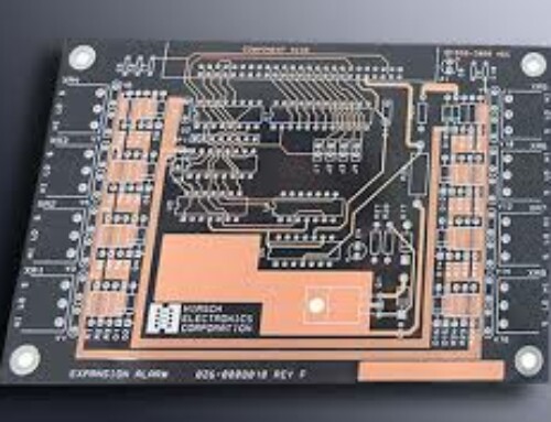
A PCB is a board used to mechanically support and electrically connect electronic components using conductive pathways, tracks, or signal traces etched from copper sheets laminated onto a non-conductive substrate. Traditional PCBs have been the backbone of electronic devices for decades, but as the demand for miniaturization and enhanced performance has grown, the limitations of conventional PCBs have become apparent.
HDI PCBs differ from traditional PCBs in several key ways.
One of the most notable differences is the use of microvias, which are significantly smaller than the vias used in standard PCBs. Microvias allow for a higher density of interconnections, enabling more complex and compact designs. This is particularly important in applications where space is at a premium, such as in smartphones, tablets, and other portable electronic devices. Additionally, HDI PCBs often incorporate multiple layers, which further increases their capacity to support intricate circuitry.
Another distinguishing feature of HDI PCBs is the use of advanced materials and manufacturing techniques.
These boards typically employ high-performance substrates and laminates that can withstand the rigors of high-speed and high-frequency applications. The manufacturing process for HDI PCBs is also more sophisticated, involving techniques such as laser drilling for microvias and sequential lamination to build up the multiple layers. These advanced processes contribute to the overall reliability and performance of HDI PCBs.
The benefits of HDI PCBs extend beyond their compact size and high wiring density.
They also offer improved electrical performance, which is crucial for high-speed and high-frequency applications. The shorter signal paths and reduced parasitic effects in HDI PCBs result in lower signal loss and better signal integrity. This makes them ideal for use in advanced communication systems, high-speed computing, and other applications where performance is critical.
Moreover, HDI PCBs contribute to the overall reliability and longevity of electronic devices.
The advanced materials and manufacturing techniques used in their production result in boards that are more robust and less prone to failure. This is particularly important in industries such as aerospace, automotive, and medical devices, where reliability is paramount.
In conclusion, HDI PCBs represent a significant advancement in the field of electronics, offering a solution to the growing demand for more compact, efficient, and high-performing electronic components. By leveraging advanced materials, manufacturing techniques, and design principles, HDI PCBs provide a platform that supports higher wiring density, improved electrical performance, and enhanced reliability. As technology continues to evolve, the importance of HDI PCBs in enabling the next generation of electronic devices cannot be overstated.

Advantages Of Using HDI PCB In Modern Electronics
High-Density Interconnect (HDI) Printed Circuit Boards (PCBs) have become a cornerstone in the advancement of modern electronics, offering a multitude of advantages that cater to the ever-evolving demands of the industry.
As electronic devices continue to shrink in size while increasing in functionality, the need for more efficient and compact circuit boards has never been more critical. HDI PCBs address this need by providing a platform that supports higher wiring density, improved electrical performance, and enhanced reliability.
One of the primary advantages of HDI PCBs is their ability to support miniaturization.
Traditional PCBs often struggle to accommodate the complex circuitry required by modern electronic devices without becoming excessively large or cumbersome. HDI technology, however, utilizes finer lines and spaces, smaller vias, and higher connection pad density, allowing for a more compact design. This miniaturization is particularly beneficial in applications such as smartphones, tablets, and wearable devices, where space is at a premium and every millimeter counts.
In addition to their compact size, HDI PCBs offer superior electrical performance.
The reduced distance between components and the use of microvias, which are smaller than traditional vias, result in lower signal loss and faster signal transmission. This is crucial in high-speed applications where signal integrity is paramount. Furthermore, the improved electrical performance of HDI PCBs contributes to better overall device performance, making them an ideal choice for advanced computing, telecommunications, and medical devices.
Another significant advantage of HDI PCBs is their enhanced reliability.
The use of microvias and blind/buried vias reduces the number of layers required in the PCB, which in turn decreases the likelihood of manufacturing defects and potential points of failure. Additionally, the materials used in HDI PCBs are often of higher quality and more robust, further contributing to their durability and longevity. This reliability is essential in critical applications such as aerospace, automotive, and industrial control systems, where failure is not an option.
The versatility of HDI PCBs also cannot be overlooked.
They are compatible with a wide range of materials and can be tailored to meet specific application requirements. This adaptability makes them suitable for a diverse array of industries and applications, from consumer electronics to military and defense systems. Moreover, the ability to integrate multiple functions into a single HDI PCB reduces the need for additional components and interconnections, simplifying the overall design and assembly process.
Cost-effectiveness is another notable benefit of HDI PCBs.
While the initial design and manufacturing costs may be higher compared to traditional PCBs, the long-term savings are substantial. The reduced size and weight of HDI PCBs lead to lower material and shipping costs. Additionally, the improved performance and reliability result in fewer failures and less need for repairs or replacements, ultimately lowering the total cost of ownership.
In conclusion, the advantages of using HDI PCBs in modern electronics are manifold. Their ability to support miniaturization, superior electrical performance, enhanced reliability, versatility, and cost-effectiveness make them an indispensable component in the development of cutting-edge electronic devices. As technology continues to advance, the role of HDI PCBs in driving innovation and meeting the demands of the industry will only become more pronounced.
Key Differences Between HDI PCB And Traditional PCB
High-Density Interconnect (HDI) Printed Circuit Boards (PCBs) represent a significant advancement in the field of electronics, offering numerous advantages over traditional PCBs. To understand the key differences between HDI PCBs and their conventional counterparts, it is essential to delve into the specific characteristics and benefits that HDI technology brings to the table.
One of the most notable differences between HDI PCBs and traditional PCBs is the density of the interconnections.
HDI PCBs are designed with a higher wiring density per unit area, which allows for more complex and compact designs. This increased density is achieved through the use of finer lines and spaces, smaller vias, and higher connection pad density. Consequently, HDI PCBs can accommodate more components in a smaller area, making them ideal for modern electronic devices that demand miniaturization without compromising functionality.
In addition to higher density, HDI PCBs employ advanced manufacturing techniques that set them apart from traditional PCBs.
For instance, HDI technology utilizes microvias, which are significantly smaller than the standard vias used in conventional PCBs. These microvias can be laser-drilled, allowing for precise placement and improved electrical performance. The use of microvias not only enhances the overall reliability of the PCB but also enables the creation of multi-layered boards with more intricate designs.
Another key difference lies in the materials used for HDI PCBs.
While traditional PCBs typically use standard FR-4 material, HDI PCBs often incorporate advanced materials such as high-performance laminates and resin-coated copper foils. These materials provide better thermal management, higher signal integrity, and improved mechanical properties, which are crucial for high-speed and high-frequency applications. As a result, HDI PCBs are better suited for demanding environments and applications where performance and reliability are paramount.
The design process for HDI PCBs also differs significantly from that of traditional PCBs.
Due to the increased complexity and higher density of HDI designs, advanced computer-aided design (CAD) tools and software are required to ensure accurate and efficient layout. Designers must consider various factors such as signal integrity, thermal management, and manufacturability during the design phase. This meticulous approach ensures that the final product meets the stringent requirements of modern electronic devices.
Furthermore, the manufacturing process for HDI PCBs involves additional steps and technologies compared to traditional PCBs.
Techniques such as sequential lamination, laser drilling, and advanced plating processes are employed to achieve the desired level of precision and performance. These additional steps contribute to the overall cost of HDI PCBs, making them more expensive than traditional PCBs. However, the benefits they offer in terms of performance, reliability, and miniaturization often justify the higher cost.
In conclusion, the key differences between HDI PCBs and traditional PCBs can be attributed to their higher interconnection density, advanced manufacturing techniques, superior materials, and more complex design and manufacturing processes. These differences enable HDI PCBs to meet the demands of modern electronic devices, offering enhanced performance, reliability, and miniaturization. As technology continues to evolve, the adoption of HDI PCBs is expected to grow, further solidifying their position as a critical component in the advancement of electronic systems.
Applications Of HDI PCB In Various Industries
High-Density Interconnect (HDI) Printed Circuit Boards (PCBs) have revolutionized the electronics industry by enabling the development of more compact, efficient, and powerful devices. These advanced PCBs are characterized by their higher wiring density per unit area, which is achieved through the use of finer lines and spaces, smaller vias, and higher connection pad density. As a result, HDI PCBs are increasingly being adopted across various industries, each leveraging the unique advantages they offer.
In the consumer electronics sector, HDI PCBs are indispensable.
The demand for smaller, lighter, and more powerful devices such as smartphones, tablets, and wearable technology has driven the need for more sophisticated circuit boards. HDI PCBs allow for the integration of more components in a limited space, enhancing the functionality and performance of these devices. For instance, the compact size of HDI PCBs enables the production of slimmer smartphones with advanced features, such as high-resolution cameras and faster processors, without compromising on battery life or durability.
Transitioning to the automotive industry, HDI PCBs play a crucial role in the development of modern vehicles.
The automotive sector is increasingly incorporating advanced electronic systems for enhanced safety, navigation, and entertainment. HDI PCBs are used in various applications, including engine control units, infotainment systems, and advanced driver-assistance systems (ADAS). The ability of HDI PCBs to support high-speed signal transmission and their reliability under harsh conditions make them ideal for automotive applications, where performance and safety are paramount.
In the medical field, the miniaturization and reliability of HDI PCBs have led to significant advancements in medical devices.
From diagnostic equipment to implantable devices, HDI PCBs are essential in creating compact and efficient medical solutions. For example, in portable medical devices such as glucose monitors and hearing aids, the small form factor of HDI PCBs allows for greater portability and ease of use. Additionally, in complex imaging systems like MRI and CT scanners, HDI PCBs contribute to the precise and reliable operation of these critical diagnostic tools.
The aerospace and defense industries also benefit significantly from the use of HDI PCBs.
In these sectors, the need for lightweight, high-performance, and reliable electronic systems is critical. HDI PCBs are used in a wide range of applications, including communication systems, navigation equipment, and control systems for aircraft and spacecraft. The ability of HDI PCBs to withstand extreme environmental conditions, such as high temperatures and vibrations, ensures their reliability in mission-critical applications. Moreover, the high-density interconnects facilitate the development of more sophisticated and compact systems, which is essential for modern aerospace and defense technologies.
Furthermore, the telecommunications industry relies heavily on HDI PCBs to meet the growing demand for faster and more reliable communication networks.
HDI PCBs are used in various telecommunications equipment, including routers, switches, and base stations. The high-speed signal transmission capabilities of HDI PCBs enable the efficient handling of large volumes of data, which is crucial for the performance of modern communication networks. As the industry continues to evolve with the advent of 5G technology, the role of HDI PCBs in supporting advanced telecommunications infrastructure becomes even more significant.
In conclusion, the applications of HDI PCBs across various industries highlight their versatility and importance in modern technology. From consumer electronics to aerospace, the unique advantages of HDI PCBs, such as their compact size, high performance, and reliability, make them an essential component in the development of advanced electronic systems. As technology continues to advance, the adoption of HDI PCBs is expected to grow, further driving innovation and efficiency across multiple sectors.