Pcb board manufacturing
Innovations In PCB Board Manufacturing Techniques
Printed Circuit Board (PCB) manufacturing has undergone significant transformations over the years, driven by the relentless pursuit of innovation and efficiency. These advancements have not only enhanced the performance and reliability of PCBs but have also streamlined the manufacturing process, making it more cost-effective and environmentally friendly.
One of the most notable innovations in PCB manufacturing is the advent of surface mount technology (SMT).
SMT has revolutionized the industry by allowing components to be mounted directly onto the surface of the PCB, as opposed to the traditional through-hole method. This technique has enabled the production of smaller, more compact boards, which are essential for modern electronic devices. Furthermore, SMT has improved the overall reliability and performance of PCBs by reducing the length of electrical paths and minimizing the risk of connection failures.
In addition to SMT, the development of advanced materials has played a crucial role in the evolution of PCB manufacturing.
High-frequency laminates, for instance, have been introduced to cater to the growing demand for high-speed and high-frequency applications. These materials exhibit superior electrical properties, such as low dielectric constant and low dissipation factor, which are essential for maintaining signal integrity in high-speed circuits. Moreover, the use of flexible and rigid-flex PCBs has gained traction in recent years, offering designers greater versatility and enabling the creation of more complex and compact electronic devices.
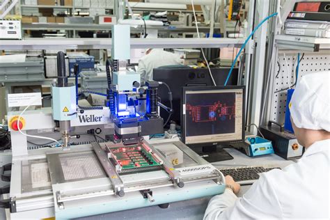
Another significant innovation in PCB manufacturing is the implementation of automated optical inspection (AOI) systems.
AOI systems have become an integral part of the quality control process, ensuring that PCBs meet stringent industry standards. By using high-resolution cameras and sophisticated algorithms, AOI systems can quickly and accurately detect defects, such as misaligned components, soldering issues, and surface contamination. This not only enhances the overall quality of the final product but also reduces the need for manual inspection, thereby increasing production efficiency.
The adoption of additive manufacturing techniques, such as 3D printing, has also made a considerable impact on PCB manufacturing.
3D printing allows for the rapid prototyping and production of complex PCB designs that would be challenging or impossible to achieve using traditional methods. This technology has opened up new possibilities for customization and innovation, enabling manufacturers to create unique and highly specialized PCBs tailored to specific applications. Additionally, 3D printing has the potential to reduce material waste and lower production costs, making it an attractive option for both small-scale and large-scale manufacturing.
Environmental sustainability has become a critical consideration in PCB manufacturing, leading to the development of eco-friendly processes and materials.
For instance, the use of lead-free solder has become increasingly common, driven by regulatory requirements and a growing awareness of the environmental and health hazards associated with lead-based solder. Furthermore, advancements in recycling techniques have made it possible to recover valuable materials from discarded PCBs, reducing the environmental impact of electronic waste.
In conclusion, the continuous innovation in PCB board manufacturing techniques has significantly enhanced the performance, reliability, and efficiency of PCBs. From surface mount technology and advanced materials to automated optical inspection systems and additive manufacturing, these advancements have transformed the industry, enabling the production of more sophisticated and environmentally friendly electronic devices. As technology continues to evolve, it is likely that we will witness even more groundbreaking developments in PCB manufacturing, further pushing the boundaries of what is possible in the world of electronics.
The Role Of Automation In Modern PCB Production
The role of automation in modern PCB production has become increasingly significant as the demand for high-quality, reliable, and cost-effective printed circuit boards (PCBs) continues to grow.
Automation has revolutionized the manufacturing process, enhancing precision, efficiency, and scalability. This transformation is driven by the need to meet the stringent requirements of various industries, including consumer electronics, automotive, aerospace, and telecommunications.
To begin with, automation in PCB manufacturing starts with the design phase, where computer-aided design (CAD) software plays a crucial role.
Engineers use CAD tools to create detailed schematics and layouts, ensuring that the design meets all specifications and standards. These digital designs are then translated into machine-readable formats, which guide automated machinery throughout the production process. This seamless transition from design to manufacturing minimizes human error and ensures consistency in the final product.
Moving forward, the fabrication of PCBs involves several automated processes, each contributing to the overall efficiency and quality of the boards.
One of the critical steps is the drilling of holes for component leads and vias, which is performed by computer-controlled drilling machines. These machines operate with remarkable precision, capable of drilling thousands of holes per minute with micron-level accuracy. This level of precision is essential for the functionality and reliability of the final product.
Subsequently, the application of conductive materials, such as copper, is another area where automation has made significant strides.
Automated plating and etching processes ensure uniform deposition of copper layers, which form the conductive pathways on the PCB. These processes are tightly controlled to achieve the desired thickness and pattern, which are critical for the electrical performance of the board. Additionally, automated inspection systems are employed to detect any defects or inconsistencies in the copper layers, further enhancing the quality control measures.
As the production process advances, the solder mask application and silkscreen printing are also automated.
Solder masks protect the copper traces from oxidation and prevent solder bridges during component assembly. Automated machines apply the solder mask with high precision, ensuring complete coverage and adherence to the design specifications. Similarly, silkscreen printing, which involves applying labels and markings on the PCB, is performed by automated printers that ensure clarity and accuracy.
Furthermore, the assembly of components onto the PCB is a highly automated process, often referred to as surface mount technology (SMT).
Automated pick-and-place machines accurately position components onto the board, guided by the digital design files. These machines can handle a wide range of component sizes and types, placing them with exceptional speed and precision. Once the components are in place, automated soldering processes, such as reflow soldering, secure them to the board, creating reliable electrical connections.
In addition to the manufacturing steps, automation plays a vital role in testing and quality assurance.
Automated optical inspection (AOI) systems and X-ray inspection machines are used to verify the integrity of solder joints, component placement, and overall board quality. These systems can quickly identify defects that may not be visible to the naked eye, ensuring that only high-quality PCBs reach the end customer.
In conclusion, the integration of automation in modern PCB production has significantly enhanced the efficiency, precision, and reliability of the manufacturing process. From design to fabrication, assembly, and testing, automated systems ensure that PCBs meet the high standards required by various industries. As technology continues to advance, the role of automation in PCB manufacturing is expected to grow even further, driving innovation and excellence in this critical field.
Environmental Impact Of PCB Manufacturing And Sustainable Practices
The environmental impact of PCB board manufacturing is a subject of growing concern as the demand for electronic devices continues to rise. Printed Circuit Boards (PCBs) are integral components in virtually all electronic devices, from smartphones to industrial machinery.
However, the manufacturing process of PCBs involves several stages that can have significant environmental repercussions. Understanding these impacts and exploring sustainable practices is crucial for mitigating the adverse effects on our planet.
The production of PCBs begins with the extraction of raw materials, such as copper, fiberglass, and various chemicals.
Mining for copper, in particular, is an energy-intensive process that results in substantial greenhouse gas emissions. Additionally, the extraction process often leads to habitat destruction and soil erosion, further exacerbating environmental degradation. Once the raw materials are obtained, they undergo various chemical treatments to form the PCB substrate. These treatments involve the use of hazardous chemicals, including acids and solvents, which can lead to soil and water contamination if not properly managed.
Moreover, the etching process, which creates the intricate circuitry on the PCB, generates a significant amount of chemical waste.
This waste often contains heavy metals and other toxic substances that pose a threat to both human health and the environment. Improper disposal of these chemicals can lead to contamination of water bodies, affecting aquatic life and potentially entering the human food chain. Furthermore, the energy consumption during the manufacturing process is considerable, contributing to the carbon footprint of PCB production.
In light of these environmental challenges, adopting sustainable practices in PCB manufacturing is imperative.
One approach is to improve the efficiency of raw material usage. For instance, recycling copper and other metals from electronic waste can reduce the need for new mining activities. This not only conserves natural resources but also minimizes the environmental impact associated with extraction processes. Additionally, implementing closed-loop systems for chemical treatments can significantly reduce waste generation. By recycling and reusing chemicals within the manufacturing process, companies can decrease the volume of hazardous waste that needs to be managed.
Another sustainable practice involves the use of alternative materials.
Researchers are exploring the potential of biodegradable substrates made from natural fibers, which can replace traditional fiberglass. These biodegradable materials can reduce the environmental footprint of PCBs by decomposing naturally at the end of their lifecycle. Furthermore, advancements in green chemistry offer the possibility of developing less toxic chemicals for use in PCB manufacturing. By substituting hazardous substances with environmentally friendly alternatives, the industry can mitigate the risks associated with chemical waste.
Energy efficiency is another critical aspect of sustainable PCB manufacturing.
Utilizing renewable energy sources, such as solar or wind power, can significantly reduce the carbon footprint of production facilities. Additionally, optimizing manufacturing processes to minimize energy consumption can further enhance sustainability. For example, adopting energy-efficient equipment and implementing best practices for energy management can lead to substantial reductions in greenhouse gas emissions.
In conclusion, while the environmental impact of PCB board manufacturing is considerable, there are numerous sustainable practices that can mitigate these effects. By improving raw material efficiency, adopting alternative materials, and enhancing energy efficiency, the industry can move towards a more sustainable future. It is essential for manufacturers, policymakers, and consumers to collaborate in promoting and implementing these practices to ensure the continued growth of the electronics industry without compromising the health of our planet.
Quality Control Measures In PCB Board Manufacturing
In the realm of PCB board manufacturing, quality control measures are paramount to ensure the reliability and functionality of the final product. The intricate nature of printed circuit boards (PCBs) necessitates a rigorous approach to quality assurance, encompassing various stages of the manufacturing process. From the initial design phase to the final inspection, each step is meticulously monitored to detect and rectify potential defects, thereby guaranteeing the highest standards of quality.
To begin with, the design phase is critical in setting the foundation for a high-quality PCB.
Design for manufacturability (DFM) principles are employed to optimize the layout, ensuring that the board can be produced efficiently and without errors. Advanced software tools are utilized to simulate the manufacturing process, identifying potential issues such as signal integrity problems, thermal management concerns, and component placement conflicts. By addressing these issues early on, manufacturers can prevent costly rework and delays later in the production cycle.
As the design transitions to the fabrication stage, stringent quality control measures are implemented to monitor the production process.
One of the key techniques used is automated optical inspection (AOI), which employs high-resolution cameras to scan the PCB for defects such as misaligned components, soldering issues, and surface irregularities. AOI systems are capable of detecting even the smallest deviations from the design specifications, allowing for immediate corrective action.
In addition to AOI, X-ray inspection is another vital tool in the quality control arsenal.
This non-destructive testing method enables manufacturers to examine the internal structure of the PCB, including hidden solder joints and vias. By providing a detailed view of the board’s internal layers, X-ray inspection helps identify defects that are not visible to the naked eye, such as voids, cracks, and insufficient solder coverage.
Electrical testing is also a crucial component of the quality control process.
This involves subjecting the PCB to a series of tests to verify its electrical performance and functionality. In-circuit testing (ICT) and flying probe testing are commonly used methods to check for open circuits, short circuits, and other electrical faults. These tests ensure that the PCB meets the required specifications and operates as intended in its final application.
Furthermore, environmental stress testing is conducted to assess the PCB’s durability and reliability under various conditions.
This includes thermal cycling, humidity testing, and vibration testing, which simulate the harsh environments that the PCB may encounter during its operational life. By exposing the board to these stressors, manufacturers can identify potential weaknesses and make necessary improvements to enhance its robustness.
Throughout the entire manufacturing process, documentation and traceability are maintained to ensure accountability and facilitate continuous improvement.
Detailed records of each production batch, including test results and inspection reports, are kept to track the performance of the PCB and identify trends or recurring issues. This data-driven approach enables manufacturers to implement corrective actions and refine their processes, ultimately leading to higher quality products.
In conclusion, quality control measures in PCB board manufacturing are essential to ensure the reliability and performance of the final product. By employing advanced inspection techniques, rigorous testing protocols, and thorough documentation practices, manufacturers can detect and address potential defects at every stage of the production process. This comprehensive approach not only enhances the quality of the PCB but also contributes to the overall success and reputation of the manufacturer in the competitive electronics industry.