Pcb sample design
Essential Tips For Creating Your First PCB Sample Design
Creating your first Printed Circuit Board (PCB) sample design can be an exciting yet challenging endeavor. To ensure a successful outcome, it is essential to follow a series of well-considered steps and best practices.
Initially, understanding the fundamental requirements of your project is crucial.
This involves defining the specifications, such as the size, shape, and functionality of the PCB. By clearly outlining these parameters, you can avoid potential pitfalls and ensure that the design meets the intended purpose.
Once the specifications are established, the next step is to select the appropriate software for designing the PCB.
There are numerous software options available, ranging from free tools like KiCad to more advanced, paid solutions such as Altium Designer. The choice of software should align with your level of expertise and the complexity of the project. Familiarizing yourself with the chosen software through tutorials and practice can significantly enhance your design efficiency and accuracy.
Transitioning from software selection to the actual design process, it is imperative to create a schematic diagram.
The schematic serves as a blueprint for the PCB, detailing the connections between various components. Ensuring that the schematic is accurate and comprehensive is vital, as any errors at this stage can lead to significant issues later in the design process. Double-checking connections and component values can save time and resources in the long run.
Following the schematic creation, the next phase involves laying out the PCB.
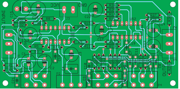
This step requires careful consideration of component placement and routing of electrical traces. Components should be strategically placed to minimize signal interference and optimize performance. Additionally, paying attention to the routing of traces is essential to prevent issues such as crosstalk and signal degradation. Utilizing design rules and guidelines provided by the software can aid in maintaining a high-quality layout.
As the layout progresses, it is also important to consider the thermal management of the PCB.
Components that generate significant heat should be placed in areas that allow for adequate heat dissipation. Incorporating thermal vias and heat sinks can further enhance the thermal performance of the PCB. Proper thermal management ensures the reliability and longevity of the final product.
Moreover, conducting a Design Rule Check (DRC) is a critical step before finalizing the PCB design.
The DRC helps identify any violations of the design rules, such as minimum trace width or spacing requirements. Addressing these issues promptly can prevent manufacturing defects and improve the overall quality of the PCB. Additionally, performing a thorough review of the design, including a visual inspection and simulation, can help identify potential problems that may not be evident through automated checks.
Once the design is finalized, the next step is to generate the necessary files for manufacturing.
These typically include Gerber files, drill files, and a Bill of Materials (BOM). Ensuring that these files are accurate and complete is essential for a smooth manufacturing process. Communicating with the manufacturer to confirm their specific requirements can further streamline this phase.
In conclusion, creating your first PCB sample design involves a series of meticulous steps, from defining specifications to generating manufacturing files. By following best practices and leveraging appropriate tools, you can achieve a successful and functional PCB design. Each phase of the process, from schematic creation to layout and thermal management, plays a crucial role in the overall quality and performance of the final product. Through careful planning and attention to detail, you can navigate the complexities of PCB design and bring your project to fruition.
Common Mistakes To Avoid In PCB Sample Design
In the realm of electronics, Printed Circuit Board (PCB) design is a critical process that demands precision and attention to detail. However, even seasoned designers can fall prey to common mistakes that can compromise the functionality and reliability of the final product.
One prevalent error is inadequate planning.
Before diving into the design phase, it is essential to thoroughly understand the requirements and constraints of the project. This includes defining the electrical specifications, mechanical constraints, and environmental conditions the PCB will be subjected to. Failing to do so can lead to design iterations and increased costs.
Another frequent mistake is poor component placement.
Components should be strategically placed to minimize signal path lengths and reduce electromagnetic interference (EMI). Placing components haphazardly can result in signal integrity issues and increased noise, which can degrade the performance of the PCB. Additionally, it is crucial to consider thermal management during component placement. Components that generate significant heat should be placed in areas with adequate ventilation or near heat sinks to prevent overheating.
Transitioning to the topic of routing, improper trace routing is another common pitfall.
Traces should be routed with care to avoid sharp angles and excessive via usage, which can introduce signal reflections and impedance mismatches. It is also important to maintain consistent trace widths to ensure uniform current distribution. Furthermore, designers should pay attention to the separation between high-speed and low-speed signals to prevent crosstalk and signal degradation.
Grounding issues are another area where mistakes frequently occur.
A solid grounding strategy is vital for the stability and performance of the PCB. Designers should avoid creating ground loops and ensure that all components have a low-impedance path to the ground plane. Inadequate grounding can lead to noise problems and erratic behavior of the circuit. Additionally, it is advisable to use a single ground plane rather than multiple ground islands to maintain signal integrity.
Moving on to the topic of design rule checks (DRCs), neglecting to perform thorough DRCs can result in manufacturability issues.
DRCs help identify potential problems such as insufficient trace clearance, solder mask slivers, and drill-to-copper violations. By rigorously adhering to DRC guidelines, designers can ensure that the PCB can be manufactured without issues and meets the required standards.
Another critical aspect to consider is the selection of materials.
Using inappropriate materials can affect the performance and durability of the PCB. For instance, choosing a substrate with a low glass transition temperature (Tg) for a high-temperature application can lead to delamination and failure. Therefore, it is essential to select materials that match the operational environment and performance requirements of the PCB.
Lastly, communication with the manufacturer is often overlookeDesigners should maintain open lines of communication with the PCB manufacturer to ensure that the design is feasible and meets the manufacturing capabilities. Providing clear and detailed documentation, including fabrication drawings and assembly instructions, can prevent misunderstandings and errors during the production process.
In conclusion, avoiding these common mistakes in PCB sample design requires a combination of careful planning, strategic component placement, meticulous routing, robust grounding, thorough design rule checks, appropriate material selection, and effective communication with the manufacturer. By addressing these areas, designers can enhance the reliability, performance, and manufacturability of their PCBs, ultimately leading to successful electronic products.
Innovative Techniques For Efficient PCB Sample Prototyping
Printed Circuit Boards (PCBs) are the backbone of modern electronic devices, serving as the foundation upon which electronic components are mounted and interconnected. The process of designing and prototyping PCBs has evolved significantly over the years, driven by the need for increased efficiency, precision, and reliability. Innovative techniques for efficient PCB sample prototyping have emerged, transforming the way engineers and designers approach the development of electronic circuits.
One of the most notable advancements in PCB sample prototyping is the adoption of computer-aided design (CAD) software.
CAD tools have revolutionized the design process by enabling engineers to create detailed and accurate PCB layouts with ease. These software solutions offer a range of features, including schematic capture, component placement, and routing optimization, which streamline the design process and reduce the likelihood of errors. Furthermore, CAD software often includes simulation capabilities, allowing designers to test and validate their designs virtually before moving on to physical prototyping.
In addition to CAD software, the use of automated manufacturing techniques has significantly improved the efficiency of PCB sample prototyping.
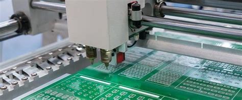
Automated machinery, such as pick-and-place machines and reflow ovens, has replaced manual assembly processes, resulting in faster production times and higher precision.
These machines are capable of placing components with remarkable accuracy, ensuring that even the most complex PCB designs can be assembled quickly and reliably. Moreover, automated manufacturing reduces the risk of human error, which can lead to costly rework and delays.
Another innovative technique that has gained traction in recent years is the use of additive manufacturing, commonly known as 3D printing, for PCB prototyping.
3D printing technology allows for the rapid production of PCB prototypes by depositing conductive and insulating materials layer by layer.
This approach offers several advantages, including the ability to create complex geometries that would be difficult or impossible to achieve with traditional manufacturing methods. Additionally, 3D printing enables rapid iteration, allowing designers to quickly produce and test multiple versions of a PCB design, ultimately leading to a more refined final product.
The integration of advanced materials into PCB prototyping has also contributed to increased efficiency and performance.
High-frequency laminates, flexible substrates, and advanced soldering materials are just a few examples of the innovative materials being used in modern PCB designs. These materials offer improved electrical performance, enhanced durability, and greater design flexibility, enabling engineers to create more sophisticated and reliable electronic devices. By leveraging these advanced materials, designers can push the boundaries of what is possible in PCB design and prototyping.
Collaboration and communication tools have also played a crucial role in enhancing the efficiency of PCB sample prototyping.
Cloud-based platforms and collaborative design environments allow teams to work together seamlessly, regardless of their physical location. These tools facilitate real-time collaboration, enabling designers to share ideas, provide feedback, and make adjustments to the design in a coordinated manner. This collaborative approach not only speeds up the prototyping process but also ensures that the final design meets the requirements and expectations of all stakeholders.
In conclusion, the landscape of PCB sample prototyping has been transformed by a range of innovative techniques that enhance efficiency, precision, and reliability. The adoption of CAD software, automated manufacturing, 3D printing, advanced materials, and collaborative tools has revolutionized the way engineers and designers approach PCB development. As technology continues to advance, it is likely that even more innovative techniques will emerge, further pushing the boundaries of what is possible in the realm of PCB design and prototyping.

The Role Of Software Tools In Modern PCB Sample Design
In the realm of modern electronics, the design of Printed Circuit Boards (PCBs) has evolved significantly, driven by the rapid advancement of software tools. These tools have become indispensable in the creation of PCB samples, facilitating a seamless transition from conceptualization to physical realization. The role of software tools in modern PCB sample design cannot be overstated, as they offer a multitude of benefits that enhance precision, efficiency, and innovation.
To begin with, software tools provide a robust platform for schematic capture, which is the initial step in PCB design.
This process involves creating a visual representation of the electronic circuit, detailing the components and their interconnections. Advanced software tools offer extensive libraries of electronic components, allowing designers to easily select and place components onto the schematic. This not only streamlines the design process but also ensures accuracy, as the software can automatically check for errors such as incorrect connections or component mismatches.
Following schematic capture, the next critical phase is the layout design.
Here, software tools play a pivotal role in translating the schematic into a physical layout that can be manufactured. These tools offer features such as automated routing, which optimizes the placement of traces to minimize signal interference and ensure efficient use of space. Additionally, they provide real-time feedback on design rules and constraints, helping designers adhere to industry standards and avoid potential issues during manufacturing.
Moreover, software tools facilitate the simulation and analysis of PCB designs, enabling designers to test and validate their circuits before committing to production.
Through simulation, designers can predict the behavior of the circuit under various conditions, identify potential problems, and make necessary adjustments. This capability is particularly valuable in complex designs where manual testing would be time-consuming and prone to errors. By leveraging simulation tools, designers can achieve higher reliability and performance in their PCB samples.
Another significant advantage of using software tools in PCB sample design is the ability to collaborate and share designs easily.
Modern software platforms often include cloud-based features that allow multiple designers to work on the same project simultaneously, regardless of their geographical location. This collaborative approach not only accelerates the design process but also fosters innovation, as team members can contribute diverse perspectives and expertise.
Furthermore, software tools support the integration of design data with manufacturing processes, ensuring a smooth transition from design to production.
They generate detailed documentation, including Gerber files, Bill of Materials (BOM), and assembly drawings, which are essential for manufacturing. This integration reduces the likelihood of errors during production and helps in maintaining consistency and quality in the final product.
In addition to these technical benefits, software tools also contribute to cost efficiency in PCB sample design. By automating various aspects of the design process, they reduce the need for manual intervention, thereby lowering labor costs. Additionally, the ability to simulate and validate designs before production minimizes the risk of costly rework and material wastage.
In conclusion, the role of software tools in modern PCB sample design is multifaceted and transformative. They enhance precision, efficiency, and collaboration, while also ensuring compliance with industry standards and facilitating seamless integration with manufacturing processes. As technology continues to advance, the capabilities of these tools are likely to expand further, driving innovation and excellence in PCB design. The adoption of sophisticated software tools is, therefore, essential for any organization aiming to stay competitive in the fast-paced world of electronics.

