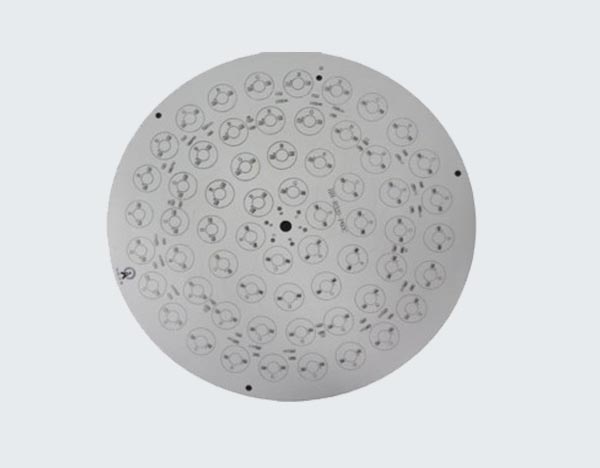
What is multilayer pcb
Introduction To Multilayer PCBs: Understanding The Basics
Multilayer printed circuit boards (PCBs) have become a cornerstone in modern electronics, offering enhanced functionality and performance compared to their single-layer and double-layer counterparts.
To understand the basics of multilayer PCBs, it is essential to delve into their structure, advantages, and applications. This exploration will provide a comprehensive overview of why multilayer PCBs are indispensable in today’s technological landscape.
At its core, a multilayer PCB consists of multiple layers of conductive material, typically copper, separated by insulating layers known as dielectric materials.
These layers are laminated together under high pressure and temperature to form a single, cohesive unit. The number of layers in a multilayer PCB can range from three to over fifty, depending on the complexity and requirements of the electronic device. The inner layers are often used for power distribution and signal routing, while the outer layers serve as the primary interface for component placement and interconnections.
One of the primary advantages of multilayer PCBs is their ability to support higher component density.
As electronic devices become more compact and sophisticated, the need for efficient use of space becomes paramount. Multilayer PCBs address this need by allowing designers to stack multiple layers of circuitry within a confined area, thereby maximizing the available real estate.
This capability is particularly beneficial in applications such as smartphones, laptops, and medical devices, where space constraints are a significant consideration.
In addition to space efficiency, multilayer PCBs offer improved electrical performance.
The close proximity of the layers reduces the length of interconnections, which in turn minimizes signal loss and electromagnetic interference (EMI). This results in faster signal transmission and enhanced overall performance. Furthermore, the use of dedicated power and ground planes within the PCB structure helps to stabilize voltage levels and reduce noise, contributing to the reliability and efficiency of the electronic device.
Another notable benefit of multilayer PCBs is their design flexibility.
The ability to incorporate multiple layers allows for more complex and intricate circuit designs, enabling the integration of advanced features and functionalities. This flexibility is crucial in industries such as aerospace, automotive, and telecommunications, where sophisticated electronic systems are required to perform critical functions. Moreover, multilayer PCBs can accommodate a wide range of materials and technologies, including high-frequency laminates and embedded components, further expanding their versatility.
Despite these advantages, the manufacturing process of multilayer PCBs is inherently more complex and costly compared to single-layer or double-layer PCBs.
The precision required in aligning and bonding multiple layers, along with the need for advanced fabrication techniques, contributes to the increased production costs. However, the benefits of enhanced performance, reliability, and space efficiency often outweigh these challenges, making multilayer PCBs a preferred choice for high-performance applications.
In conclusion, multilayer PCBs represent a significant advancement in the field of electronics, offering numerous benefits that cater to the demands of modern technology.
Their ability to support higher component density, improve electrical performance, and provide design flexibility makes them an essential component in a wide array of applications. As technology continues to evolve, the role of multilayer PCBs is likely to become even more critical, driving innovation and enabling the development of increasingly sophisticated electronic devices. Understanding the basics of multilayer PCBs is therefore fundamental for anyone involved in the design, manufacturing, or utilization of advanced electronic systems.

Advantages Of Using Multilayer PCBs In Modern Electronics
Multilayer printed circuit boards (PCBs) have become a cornerstone in the design and manufacturing of modern electronic devices. These advanced PCBs consist of multiple layers of conductive material separated by insulating layers, all laminated together into a single, compact structure. The advantages of using multilayer PCBs in contemporary electronics are numerous, making them an indispensable component in a wide range of applications.
One of the primary benefits of multilayer PCBs is their ability to support higher component density.
As electronic devices become increasingly complex and compact, the need for more components within a limited space has grown. Multilayer PCBs address this challenge by providing multiple layers for component placement and interconnections, thereby maximizing the use of available space.
This increased density not only allows for more functionality within a smaller footprint but also contributes to the miniaturization of electronic devices, a trend that is particularly evident in consumer electronics such as smartphones, tablets, and wearable technology.
In addition to supporting higher component density, multilayer PCBs offer enhanced electrical performance.
The multiple layers enable designers to create more intricate and efficient routing paths for electrical signals. This results in reduced signal interference and crosstalk, which are critical factors in maintaining signal integrity, especially in high-speed and high-frequency applications. Furthermore, the ability to incorporate ground and power planes within the layers helps to stabilize voltage levels and reduce electromagnetic interference (EMI), leading to improved overall performance and reliability of the electronic device.
Another significant advantage of multilayer PCBs is their inherent design flexibility.
The multiple layers provide ample opportunities for designers to implement complex circuit designs that would be impossible or impractical with single-layer or double-layer PCBs. This flexibility is particularly beneficial in applications that require sophisticated functionality, such as advanced computing systems, telecommunications equipment, and medical devices. By leveraging the capabilities of multilayer PCBs, designers can create more innovative and efficient solutions that meet the demanding requirements of these advanced applications.
Moreover, multilayer PCBs contribute to improved thermal management in electronic devices.
As electronic components become more powerful, they generate more heat, which can adversely affect performance and longevity. The layered structure of multilayer PCBs allows for better heat dissipation, as heat can be distributed across multiple layers and away from critical components. This enhanced thermal management is essential for maintaining the reliability and efficiency of high-performance electronic devices, particularly in industries such as aerospace, automotive, and industrial automation.

The robustness and durability of multilayer PCBs also make them a preferred choice in many applications.
The laminated structure provides added mechanical strength, making these PCBs more resistant to bending, vibration, and other physical stresses. This durability is crucial in environments where electronic devices are subjected to harsh conditions, such as in military and aerospace applications. The reliability of multilayer PCBs ensures that electronic systems can operate effectively and consistently, even in challenging environments.
In conclusion, the advantages of using multilayer PCBs in modern electronics are manifold. Their ability to support higher component density, enhance electrical performance, offer design flexibility, improve thermal management, and provide robustness and durability makes them an essential component in the development of advanced electronic devices. As technology continues to evolve, the role of multilayer PCBs in enabling innovation and driving progress in the electronics industry will undoubtedly remain significant.
Manufacturing Process Of Multilayer PCBs: Step-By-Step Guide
The manufacturing process of multilayer printed circuit boards (PCBs) is a complex and meticulous procedure that requires precision and expertise. Multilayer PCBs, which consist of multiple layers of conductive material separated by insulating layers, are essential in modern electronics due to their ability to support high-density circuits. The process begins with the design phase, where engineers use specialized software to create a detailed blueprint of the PCB. This design includes the layout of the circuits, the placement of components, and the routing of electrical connections.
Once the design is finalized, the next step is to create the individual layers of the PCB.
This involves selecting the appropriate materials, typically a combination of copper and insulating substrates such as fiberglass-reinforced epoxy. The copper is laminated onto the substrate to form the conductive layers. Each layer is then coated with a photosensitive material, which is exposed to ultraviolet light through a photomask that corresponds to the circuit design. The exposed areas of the photosensitive material harden, while the unexposed areas remain soft and are subsequently removed, leaving behind the desired circuit pattern.
Following the creation of the individual layers, the next phase is the alignment and lamination process.
The layers are carefully aligned to ensure that the circuits on each layer match up correctly. This is a critical step, as any misalignment can result in faulty connections and a non-functional PCB. Once aligned, the layers are laminated together under high pressure and temperature, which fuses them into a single, solid board.
After lamination, the PCB undergoes drilling to create holes for the electrical connections between layers, known as vias.
These holes are drilled using precision machinery to ensure accuracy. The drilled holes are then plated with copper to establish the necessary electrical connections. This plating process involves depositing a thin layer of copper onto the walls of the holes, which is achieved through electroplating.
The next step is the application of the solder mask, which is a protective layer that covers the entire surface of the PCB except for the areas where components will be soldered. The solder mask prevents short circuits and protects the copper traces from oxidation and other environmental factors. It is applied as a liquid and then cured using ultraviolet light.
Following the application of the solder mask, the PCB undergoes a process called silkscreening.
This involves printing labels, symbols, and other markings onto the board to aid in the assembly and identification of components. The silkscreen is typically applied using a stencil and ink, which is then cured to ensure durability.
The final steps in the manufacturing process include the application of a surface finish and electrical testing.
The surface finish, such as gold or silver, is applied to the exposed copper areas to enhance solderability and protect against corrosion. Electrical testing is conducted to verify that the PCB functions correctly and that there are no short circuits or open connections. This testing is crucial to ensure the reliability and performance of the final product.
In conclusion, the manufacturing process of multilayer PCBs involves a series of precise and carefully controlled steps, from design and material selection to lamination, drilling, and testing. Each phase is critical to producing a high-quality PCB that meets the stringent requirements of modern electronic devices. The complexity and precision required in this process highlight the importance of expertise and advanced technology in the production of multilayer PCBs.
Common Applications Of Multilayer PCBs In Various Industries
Multilayer printed circuit boards (PCBs) have become a cornerstone in modern electronics, offering enhanced functionality and compact design. These advanced PCBs consist of multiple layers of conductive material separated by insulating layers, allowing for more complex and efficient circuitry. The versatility and efficiency of multilayer PCBs have led to their widespread adoption across various industries, each leveraging their unique benefits to meet specific technological demands.
In the telecommunications industry, multilayer PCBs are indispensable.
The need for high-speed data transmission and reliable connectivity has driven the development of sophisticated communication devices. Multilayer PCBs support the intricate circuitry required for smartphones, routers, and satellite systems, ensuring robust performance and minimal signal interference. Their ability to handle high-frequency signals and reduce electromagnetic interference makes them ideal for these applications, where precision and reliability are paramount.
The medical field also heavily relies on multilayer PCBs, particularly in diagnostic and monitoring equipment.
Devices such as MRI machines, CT scanners, and portable medical devices require compact and highly reliable circuit boards to function effectively. Multilayer PCBs provide the necessary miniaturization and reliability, enabling the development of advanced medical technologies that can deliver accurate diagnostics and patient monitoring. Furthermore, the stringent regulatory standards in the medical industry necessitate the use of high-quality, dependable components, making multilayer PCBs a preferred choice.
In the realm of consumer electronics, the demand for smaller, more powerful devices has driven the adoption of multilayer PCBs.
From laptops and tablets to gaming consoles and wearable technology, these PCBs allow manufacturers to pack more functionality into increasingly compact designs. The ability to integrate multiple layers of circuitry within a single board not only saves space but also enhances the overall performance and durability of consumer electronic products. This trend towards miniaturization and enhanced functionality continues to push the boundaries of what is possible in consumer electronics.
The automotive industry is another sector where multilayer PCBs play a crucial role.
Modern vehicles are equipped with a plethora of electronic systems, including advanced driver-assistance systems (ADAS), infotainment systems, and engine control units (ECUs). Multilayer PCBs are essential in these applications due to their ability to support complex circuitry and withstand harsh operating conditions. The automotive industry’s push towards electric and autonomous vehicles further underscores the importance of reliable and efficient multilayer PCBs, as these technologies require sophisticated electronic control systems.
Aerospace and defense applications also benefit significantly from multilayer PCBs.
The stringent requirements for reliability, performance, and durability in these sectors necessitate the use of advanced PCB technology. Multilayer PCBs are used in a wide range of aerospace and defense equipment, from avionics and radar systems to communication satellites and missile guidance systems. Their ability to operate reliably under extreme conditions and their high-density interconnect capabilities make them ideal for these critical applications.
In conclusion, multilayer PCBs have become integral to various industries, each leveraging their unique advantages to meet specific technological needs. The telecommunications, medical, consumer electronics, automotive, and aerospace sectors all benefit from the enhanced functionality, reliability, and compact design that multilayer PCBs offer. As technology continues to advance, the demand for sophisticated and efficient circuit solutions will only grow, further cementing the importance of multilayer PCBs in the modern technological landscape.

