What is pad in pcb
Introduction To Pad In PCB Design
In the realm of printed circuit board (PCB) design, the term “pad” holds significant importance. A pad in PCB design refers to the small, conductive areas on the board where components are soldered.
These pads serve as the critical interface between the electronic components and the PCB itself, ensuring electrical connectivity and mechanical stability. Understanding the role and design considerations of pads is essential for anyone involved in PCB design and manufacturing.
Pads come in various shapes and sizes, each tailored to accommodate different types of components and their specific requirements.
Typically, pads are circular or rectangular, but they can also be designed in more complex shapes to fit unique component leads. The size and shape of a pad are determined by several factors, including the type of component, the method of assembly, and the electrical and mechanical requirements of the circuit. For instance, surface-mount technology (SMT) components require different pad designs compared to through-hole components.
One of the primary functions of a pad is to provide a secure and reliable point of attachment for components.
This is achieved through the process of soldering, where the component leads are bonded to the pads using solder. The quality of this bond is crucial, as it affects the overall performance and reliability of the PCB. Poorly designed or improperly manufactured pads can lead to weak solder joints, which may result in intermittent connections or complete failure of the circuit.
In addition to providing a mechanical anchor, pads also play a vital role in ensuring electrical connectivity.
They act as the interface between the component leads and the copper traces on the PCB, allowing electrical signals to flow seamlessly through the circuit. The electrical performance of a pad is influenced by its size, shape, and the quality of the solder joint. Therefore, careful consideration must be given to these factors during the design phase to ensure optimal performance.
Thermal management is another critical aspect of pad design.
During the soldering process, heat is applied to melt the solder and create a bond between the component lead and the pad. If the pad is too small or poorly designed, it may not dissipate heat effectively, leading to overheating and potential damage to the component or the PCB. Conversely, if the pad is too large, it may absorb too much heat, making it difficult to achieve a proper solder joint. Therefore, achieving the right balance in pad design is essential for effective thermal management.
Moreover, the placement and arrangement of pads on a PCB must be carefully planned to avoid issues such as solder bridging and tombstoning.
Solder bridging occurs when excess solder creates an unintended connection between adjacent pads, leading to short circuits. Tombstoning, on the other hand, happens when one end of a component lifts off the pad during soldering, resulting in an incomplete connection. Both issues can be mitigated through meticulous pad design and layout planning.
In conclusion, pads are fundamental elements in PCB design, serving as the critical points of attachment and electrical connectivity for components. Their design and placement require careful consideration to ensure mechanical stability, electrical performance, and effective thermal management. By understanding the intricacies of pad design, engineers can create reliable and high-performing PCBs that meet the demands of modern electronic applications.
Types Of Pads Used In PCB Manufacturing
In the realm of printed circuit board (PCB) manufacturing, the term “pad” refers to the small, flat, and typically round or square areas of metal on the PCB where components are soldered. These pads are crucial for establishing electrical connections between the components and the conductive traces on the board. Understanding the different types of pads used in PCB manufacturing is essential for anyone involved in the design and production of electronic circuits.
One of the most common types of pads is the through-hole pad.
These pads are designed for components with leads that pass through the board. The through-hole pad consists of a hole surrounded by a ring of metal, known as the annular ring. The component lead is inserted into the hole and soldered to the annular ring, creating a secure mechanical and electrical connection. Through-hole pads are often used in applications where strong mechanical bonds are required, such as in connectors and large components.
In contrast, surface mount pads are used for surface mount technology (SMT) components, which are placed directly onto the surface of the PCB.
These pads do not have holes; instead, they are flat areas of metal where the component leads or terminals are soldered. Surface mount pads come in various shapes and sizes, depending on the type of component they are designed to accommodate. For instance, rectangular pads are commonly used for resistors and capacitors, while more complex shapes may be used for integrated circuits and other multi-lead components. Surface mount technology allows for higher component density and more compact PCB designs, making it ideal for modern electronic devices.
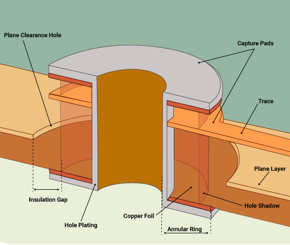
Another important type of pad is the via pad. Vias are small holes that connect different layers of a multi-layer PCB.
Via pads are the metal areas around these holes, providing a connection point for the conductive traces on each layer. There are several types of vias, including through-hole vias, blind vias, and buried vias. Through-hole vias pass through the entire thickness of the PCB, while blind vias connect an outer layer to one or more inner layers without going through the entire board. Buried vias, on the other hand, connect only inner layers and are not visible from the outer layers. Via pads are essential for creating complex, multi-layer PCB designs that require interconnections between different layers.
Additionally, there are thermal pads, which are used to dissipate heat from high-power components.
These pads are typically larger and may be connected to a heat sink or a large copper area on the PCB to help spread and dissipate heat. Proper thermal management is crucial for maintaining the reliability and performance of electronic devices, especially those with high power consumption.
Furthermore, fiducial pads are used as reference points for automated assembly machines.
These pads are not used for electrical connections but serve as alignment markers to ensure precise placement of components during the assembly process. Fiducial pads are usually placed at strategic locations on the PCB to provide accurate reference points for the assembly equipment.
In conclusion, the various types of pads used in PCB manufacturing each serve specific purposes, from providing mechanical and electrical connections to aiding in thermal management and assembly precision. Through-hole pads, surface mount pads, via pads, thermal pads, and fiducial pads all play vital roles in the design and functionality of printed circuit boards. Understanding these different types of pads is essential for anyone involved in PCB design and manufacturing, as it ensures the creation of reliable and efficient electronic devices.
Importance Of Pad Placement In PCB Layout
In the realm of printed circuit board (PCB) design, the placement of pads is a critical aspect that significantly influences the overall functionality and reliability of the final product. Pads, which are the conductive areas on a PCB where components are soldered, serve as the crucial interface between the electronic components and the board itself. Proper pad placement is essential for ensuring robust electrical connections, facilitating efficient manufacturing processes, and enhancing the durability of the PCB.
To begin with, the strategic placement of pads is vital for maintaining the electrical integrity of the circuit.
Pads must be positioned in a manner that minimizes signal interference and ensures optimal current flow. Poorly placed pads can lead to issues such as signal crosstalk, electromagnetic interference (EMI), and increased resistance, all of which can degrade the performance of the PCB. By carefully considering the electrical characteristics of the circuit and the layout of the components, designers can place pads in locations that promote stable and reliable electrical connections.
Moreover, pad placement plays a significant role in the manufacturability of the PCB.
During the assembly process, components are soldered onto the pads, and the precision of this operation is heavily dependent on the accuracy of pad placement. Misaligned pads can result in soldering defects such as cold joints, bridges, and tombstoning, which can compromise the functionality of the PCB. To mitigate these risks, designers must adhere to industry standards and guidelines for pad placement, ensuring that pads are correctly aligned with the corresponding component leads and that there is sufficient spacing between adjacent pads to prevent solder bridging.
In addition to electrical and manufacturing considerations, the placement of pads also impacts the mechanical stability and durability of the PCB.
Pads that are placed too close to the edges of the board or in areas subject to mechanical stress can lead to issues such as pad lifting, cracking, and delamination. These mechanical failures can be particularly problematic in applications where the PCB is exposed to harsh environmental conditions or mechanical vibrations. By strategically placing pads in areas that are less prone to mechanical stress and by using appropriate pad sizes and shapes, designers can enhance the mechanical robustness of the PCB.
Furthermore, the placement of pads must also take into account thermal management considerations.
Components that generate significant amounts of heat, such as power transistors and voltage regulators, require pads that can effectively dissipate heat to prevent overheating and ensure reliable operation. Thermal vias and heat sinks can be incorporated into the pad design to facilitate heat dissipation, but their effectiveness is contingent on the proper placement of the pads. By optimizing pad placement for thermal management, designers can improve the thermal performance of the PCB and extend the lifespan of the components.
In conclusion, the importance of pad placement in PCB layout cannot be overstated. It is a multifaceted aspect of PCB design that influences electrical performance, manufacturability, mechanical stability, and thermal management. By carefully considering these factors and adhering to best practices for pad placement, designers can create PCBs that are not only functional and reliable but also capable of withstanding the demands of their intended applications. As technology continues to advance and the complexity of electronic devices increases, the significance of meticulous pad placement in PCB design will only continue to grow.
Common Issues And Solutions For PCB Pad Design
Printed Circuit Boards (PCBs) are the backbone of modern electronic devices, and the design of PCB pads is a critical aspect that can significantly impact the performance and reliability of the final product. A PCB pad is a small, flat, conductive area on the board where components are soldered.
These pads serve as the interface between the electronic components and the PCB, ensuring electrical connectivity and mechanical stability. However, designing PCB pads is not without its challenges. Common issues can arise, but understanding these problems and their solutions can lead to more robust and reliable PCB designs.
One prevalent issue in PCB pad design is insufficient pad size.
Pads that are too small can lead to poor solder joints, which may result in intermittent connections or complete failure of the component. To address this, designers should adhere to industry standards and guidelines, such as those provided by the IPC (Institute for Printed Circuits). Ensuring that pads are appropriately sized for the components they will support is crucial for achieving reliable solder joints.
Another common problem is the misalignment of pads.
Misaligned pads can cause components to be improperly placed, leading to assembly issues and potential short circuits. To mitigate this, designers should use precise layout tools and double-check the alignment of pads during the design process. Additionally, employing automated optical inspection (AOI) systems during manufacturing can help detect and correct misalignments before they become problematic.
Thermal management is also a significant concern in PCB pad design.
Pads that are not adequately designed to dissipate heat can lead to overheating of components, which can reduce their lifespan or cause them to fail. To solve this issue, designers can incorporate thermal vias, which are small holes filled with conductive material that help transfer heat away from the pad. Additionally, using larger pads or adding heat sinks can further improve thermal management.
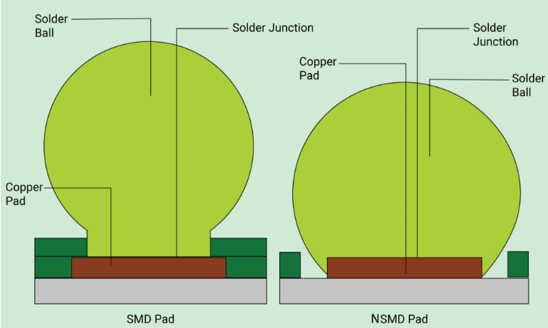
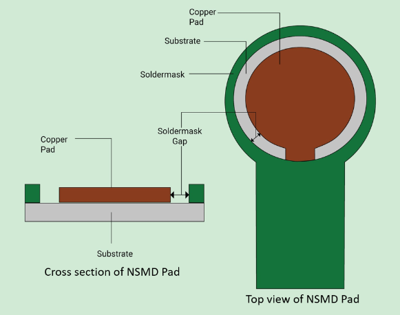
Solder mask design is another area where issues can arise.
The solder mask is a protective layer that prevents solder from bridging between pads and causing short circuits. However, if the solder mask is not properly aligned or if there are gaps, it can lead to solder bridging. To prevent this, designers should ensure that the solder mask openings are correctly sized and aligned with the pads. Using a solder mask defined (SMD) pad design, where the solder mask opening is slightly smaller than the pad, can also help reduce the risk of solder bridging.
Furthermore, the choice of pad finish can impact the reliability of the solder joints.
Common finishes include HASL (Hot Air Solder Leveling), ENIG (Electroless Nickel Immersion Gold), and OSP (Organic Solderability Preservative). Each finish has its advantages and disadvantages, and the choice should be based on the specific requirements of the application. For instance, ENIG provides a flat surface and excellent solderability, making it suitable for fine-pitch components, while HASL is more cost-effective but may not be ideal for high-density designs.
In conclusion, while PCB pad design presents several challenges, understanding common issues and their solutions can lead to more reliable and efficient designs. By ensuring proper pad size, alignment, thermal management, solder mask design, and pad finish, designers can mitigate potential problems and enhance the performance and longevity of the final product. As technology continues to advance, staying informed about best practices and industry standards will be essential for successful PCB pad design.