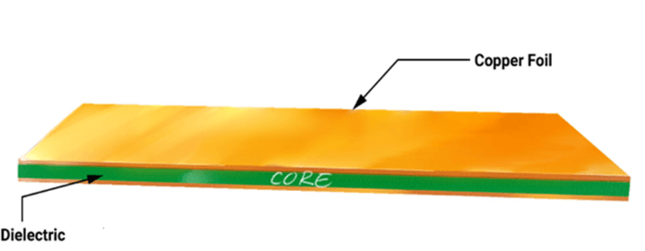
Pcb copper clad laminate
Benefits Of Using High-Quality Copper Clad Laminate In PCB Manufacturing
In the realm of printed circuit board (PCB) manufacturing, the choice of materials plays a pivotal role in determining the performance, reliability, and longevity of the final product. Among these materials, copper clad laminate (CCL) stands out as a fundamental component. High-quality copper clad laminate offers a multitude of benefits that significantly enhance the overall efficacy of PCBs, making it an indispensable choice for manufacturers aiming to produce superior electronic devices.
To begin with, high-quality copper clad laminate ensures excellent electrical conductivity, which is crucial for the efficient functioning of PCBs.
The copper layer in the laminate acts as a conductive path for electrical signals, facilitating seamless communication between various components on the board. This high conductivity minimizes signal loss and ensures that electronic devices operate at optimal performance levels. Consequently, devices manufactured with superior CCL exhibit enhanced speed and reliability, which is particularly important in high-frequency applications such as telecommunications and computing.
Moreover, the thermal management properties of high-quality copper clad laminate cannot be overstated.
Electronic components generate heat during operation, and effective heat dissipation is essential to prevent overheating and potential damage. High-quality CCLs are designed to offer excellent thermal conductivity, allowing heat to be efficiently transferred away from critical components. This thermal management capability not only extends the lifespan of the PCB but also ensures consistent performance, even under demanding conditions. As a result, devices incorporating high-quality CCLs are more robust and dependable.
In addition to electrical and thermal advantages, high-quality copper clad laminate also provides superior mechanical strength and durability.
The laminate’s robust construction ensures that the PCB can withstand physical stresses during manufacturing, assembly, and operation. This durability is particularly important in applications where the PCB may be subjected to mechanical vibrations, shocks, or other environmental factors. By using high-quality CCL, manufacturers can produce PCBs that maintain their structural integrity and functionality over extended periods, thereby reducing the likelihood of failures and the need for costly repairs or replacements.
Furthermore, high-quality copper clad laminate contributes to improved signal integrity, which is essential for maintaining the accuracy and reliability of electronic signals.
The uniformity and consistency of the copper layer in high-quality CCLs help to minimize signal distortion and interference, ensuring that signals are transmitted with high fidelity. This is especially critical in applications where precise signal transmission is paramount, such as in medical devices, aerospace, and automotive electronics. By ensuring high signal integrity, high-quality CCLs enable the development of advanced electronic systems that meet stringent performance standards.
Another significant benefit of using high-quality copper clad laminate is its compatibility with advanced manufacturing processes.
High-quality CCLs are designed to be compatible with various fabrication techniques, including surface mount technology (SMT) and through-hole technology (THT). This versatility allows manufacturers to employ the most suitable production methods for their specific requirements, resulting in efficient and cost-effective manufacturing processes. Additionally, high-quality CCLs often exhibit excellent adhesion properties, ensuring that components are securely attached to the PCB, further enhancing the reliability of the final product.
In conclusion, the use of high-quality copper clad laminate in PCB manufacturing offers a myriad of benefits that collectively contribute to the production of superior electronic devices. From excellent electrical and thermal conductivity to enhanced mechanical strength and signal integrity, high-quality CCLs provide the foundation for reliable, high-performance PCBs. By investing in high-quality materials, manufacturers can ensure that their products meet the rigorous demands of modern electronic applications, ultimately leading to greater customer satisfaction and market success.
Innovations In Copper Clad Laminate Materials For Advanced PCBs
Copper clad laminate (CCL) materials are fundamental to the construction of printed circuit boards (PCBs), serving as the substrate upon which electronic components are mounted. As the demand for more advanced and efficient electronic devices continues to grow, innovations in CCL materials have become increasingly critical. These advancements are driven by the need for higher performance, greater reliability, and enhanced functionality in a wide range of applications, from consumer electronics to aerospace and medical devices.
One of the most significant innovations in CCL materials is the development of high-frequency laminates.
Traditional CCLs, typically composed of woven glass fabric impregnated with epoxy resin and clad with copper foil, are often insufficient for high-frequency applications due to their dielectric properties. High-frequency laminates, on the other hand, are designed to minimize signal loss and maintain signal integrity at higher frequencies. These materials often incorporate advanced resins, such as polytetrafluoroethylene (PTFE) or hydrocarbon-based resins, which offer lower dielectric constants and dissipation factors. Consequently, they are ideal for applications in telecommunications, radar systems, and high-speed digital circuits.
In addition to high-frequency laminates, there has been considerable progress in the development of thermally conductive CCLs.
As electronic devices become more powerful and compact, effective thermal management is crucial to prevent overheating and ensure long-term reliability. Thermally conductive CCLs incorporate materials such as ceramic fillers or metal cores to enhance heat dissipation. These laminates are particularly beneficial in power electronics, LED lighting, and automotive applications, where efficient thermal management is essential for optimal performance and longevity.
Another area of innovation is the creation of environmentally friendly CCLs.
With increasing awareness of environmental issues and stricter regulations on hazardous substances, the electronics industry is under pressure to adopt more sustainable practices. Lead-free and halogen-free CCLs have been developed to address these concerns. These materials eliminate the use of toxic substances, such as lead and halogenated flame retardants, without compromising performance. This shift towards greener materials not only helps manufacturers comply with environmental regulations but also aligns with the growing consumer demand for eco-friendly products.
Moreover, advancements in flexible CCLs have opened new possibilities for the design and functionality of electronic devices.
Flexible CCLs, made from materials like polyimide or polyester, allow for the creation of flexible and foldable PCBs. These laminates are essential for applications where space constraints and mechanical flexibility are critical, such as in wearable electronics, flexible displays, and medical devices. The ability to bend and conform to various shapes without losing electrical performance significantly expands the design possibilities for engineers and designers.
Furthermore, the integration of advanced manufacturing techniques, such as laser direct structuring (LDS) and additive manufacturing, has further enhanced the capabilities of CCL materials.
These techniques enable the precise and efficient creation of complex circuit patterns directly on the laminate surface, reducing the need for traditional etching processes and minimizing material waste. This not only improves manufacturing efficiency but also allows for greater design flexibility and the production of more intricate and compact PCBs.
In conclusion, the continuous innovation in copper clad laminate materials is pivotal to the advancement of modern electronics. High-frequency laminates, thermally conductive CCLs, environmentally friendly options, flexible laminates, and advanced manufacturing techniques are all contributing to the development of more efficient, reliable, and versatile PCBs. As technology continues to evolve, these innovations will play a crucial role in meeting the ever-growing demands of various industries, paving the way for the next generation of electronic devices.
Environmental Impact Of Copper Clad Laminate Production And Disposal
The production and disposal of copper clad laminate (CCL), a fundamental material in the manufacturing of printed circuit boards (PCBs), have significant environmental implications. As the demand for electronic devices continues to surge, understanding the environmental impact of CCL is crucial for developing sustainable practices within the electronics industry.
To begin with, the production of copper clad laminate involves several stages, each contributing to environmental degradation.
The primary materials used in CCL are copper foil and a substrate, typically made from fiberglass reinforced epoxy resin. The extraction and processing of copper ore are energy-intensive activities that result in substantial greenhouse gas emissions. Additionally, the mining process often leads to habitat destruction, soil erosion, and water pollution due to the release of toxic substances such as heavy metals and sulfuric acid.
Moreover, the production of the epoxy resin substrate also poses environmental challenges.
Epoxy resins are derived from petrochemicals, which are non-renewable resources. The manufacturing process involves the use of hazardous chemicals, including bisphenol-A (BPA) and epichlorohydrin, both of which are associated with health risks and environmental toxicity. The release of volatile organic compounds (VOCs) during the production of epoxy resins contributes to air pollution and poses risks to human health.
In addition to the environmental impact of raw material extraction and processing, the manufacturing of CCL itself generates waste and emissions.
The lamination process, which involves bonding the copper foil to the substrate, requires high temperatures and pressures, consuming significant amounts of energy. The etching process, used to create the desired circuit patterns on the copper surface, involves the use of strong acids and generates hazardous waste, including spent etching solutions and copper sludge. Proper disposal and treatment of these wastes are essential to prevent soil and water contamination.
Furthermore, the disposal of electronic waste (e-waste) containing CCL presents another set of environmental challenges.
E-waste is one of the fastest-growing waste streams globally, and improper disposal can lead to severe environmental and health consequences. When CCL-containing e-waste is discarded in landfills, the copper and other hazardous materials can leach into the soil and groundwater, causing contamination. Incineration of e-waste, on the other hand, releases toxic fumes and heavy metals into the atmosphere, contributing to air pollution and posing risks to human health.
To mitigate the environmental impact of CCL production and disposal, several strategies can be employed.
Firstly, adopting more sustainable mining practices and improving the efficiency of copper extraction can reduce the environmental footprint of raw material procurement. Secondly, the development and use of alternative, eco-friendly materials for the substrate, such as bio-based resins, can decrease reliance on petrochemicals and reduce the release of harmful substances. Additionally, implementing cleaner production techniques and improving waste management practices in CCL manufacturing can minimize emissions and hazardous waste generation.
Recycling and proper disposal of e-waste are also critical in addressing the environmental impact of CCL.
Establishing robust e-waste collection and recycling programs can ensure that valuable materials, including copper, are recovered and reused, reducing the need for new raw materials and minimizing environmental contamination. Public awareness and education on the importance of responsible e-waste disposal can further enhance the effectiveness of these programs.
In conclusion, while the production and disposal of copper clad laminate are integral to the electronics industry, they pose significant environmental challenges. By adopting sustainable practices and improving waste management, it is possible to mitigate these impacts and move towards a more environmentally responsible approach to CCL production and disposal.
Comparing Different Types Of Copper Clad Laminates For Specific PCB Applications
When selecting the appropriate copper clad laminate (CCL) for specific printed circuit board (PCB) applications, it is essential to understand the various types available and their distinct properties. Copper clad laminates serve as the foundational material for PCBs, providing both the structural support and the conductive pathways necessary for electronic functionality. The choice of CCL can significantly impact the performance, reliability, and cost-effectiveness of the final product. Therefore, a comprehensive comparison of different types of CCLs is crucial for making informed decisions.
One of the most commonly used types of copper clad laminates is the FR-4 laminate, which is composed of woven fiberglass cloth with an epoxy resin binder.
FR-4 is renowned for its excellent mechanical strength, good electrical insulation properties, and moderate cost. These characteristics make it a versatile choice for a wide range of applications, from consumer electronics to industrial equipment. However, FR-4 may not be suitable for high-frequency applications due to its relatively high dielectric constant and loss tangent.
For high-frequency applications, materials such as PTFE (polytetrafluoroethylene) laminates are often preferred.
PTFE laminates, commonly known by the brand name Teflon, offer superior electrical properties, including a low dielectric constant and low loss tangent. These properties make PTFE laminates ideal for RF (radio frequency) and microwave circuits, where signal integrity is paramount. Despite their excellent performance, PTFE laminates are more expensive and can be challenging to process, requiring specialized manufacturing techniques.
In addition to FR-4 and PTFE, there are other specialized laminates designed for specific applications.
For instance, polyimide laminates are known for their exceptional thermal stability and chemical resistance. These properties make polyimide laminates suitable for high-temperature environments and applications where exposure to harsh chemicals is expected. Polyimide laminates are often used in aerospace, military, and automotive industries, where reliability under extreme conditions is critical.
Another important category of copper clad laminates is metal-backed laminates
which incorporate a metal substrate, such as aluminum or copper, to enhance thermal management. These laminates are particularly useful in power electronics and LED lighting applications, where efficient heat dissipation is essential to prevent overheating and ensure longevity. Metal-backed laminates provide a robust solution for managing thermal challenges, although they may add weight and complexity to the PCB design.
Furthermore, environmentally friendly laminates, such as halogen-free and lead-free options, are gaining popularity due to increasing regulatory requirements and consumer demand for sustainable products.
Halogen-free laminates eliminate the use of halogenated flame retardants, reducing the release of toxic gases during combustion. Lead-free laminates comply with RoHS (Restriction of Hazardous Substances) directives, ensuring that electronic products are safer for both users and the environment. These eco-friendly laminates offer comparable performance to traditional materials while supporting sustainability goals.
In conclusion, the selection of copper clad laminates for specific PCB applications involves careful consideration of various factors, including electrical properties, thermal performance, mechanical strength, and environmental impact. By understanding the unique characteristics of different types of CCLs, designers and engineers can make informed choices that optimize the performance and reliability of their electronic products. Whether prioritizing signal integrity, thermal management, or sustainability, the right copper clad laminate can significantly enhance the overall effectiveness of a PCB, ensuring it meets the demands of its intended application.