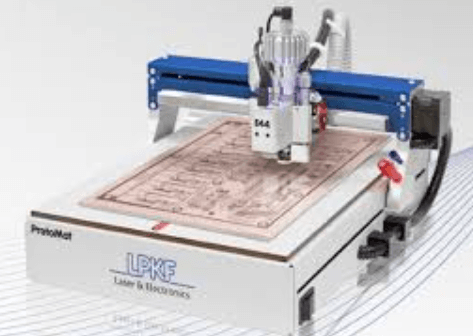
Prototype pcb board
Benefits Of Using Prototype PCB Boards In Product Development
Prototype PCB boards play a crucial role in the realm of product development, offering a multitude of benefits that significantly enhance the design and testing phases of electronic products.
One of the primary advantages of using prototype PCB boards is the ability to validate and refine designs before committing to full-scale production.
This early-stage testing allows engineers to identify and rectify potential issues, thereby reducing the risk of costly errors and ensuring that the final product meets the desired specifications.
Moreover, prototype PCB boards facilitate rapid iteration, enabling designers to experiment with different configurations and components. This flexibility is particularly valuable in the fast-paced world of technology, where innovation and adaptability are key. By allowing for quick modifications, prototype PCB boards help teams to stay agile and responsive to changing requirements or new insights that may emerge during the development process.
In addition to enhancing design accuracy and flexibility, prototype PCB boards also contribute to cost efficiency.
By identifying and addressing design flaws early on, companies can avoid the expenses associated with reworking or scrapping defective products. Furthermore, the use of prototype PCB boards can streamline the production process by providing a clear and tested blueprint for mass manufacturing. This not only reduces the likelihood of production delays but also ensures a smoother transition from prototype to final product.
Another significant benefit of prototype PCB boards is their role in improving communication and collaboration among team members.
By providing a tangible representation of the design, these boards enable engineers, designers, and stakeholders to better visualize and understand the product. This shared understanding can facilitate more effective discussions, leading to more informed decision-making and a more cohesive development process.
Additionally, prototype PCB boards can serve as valuable tools for demonstrating concepts to potential investors or clients. A physical prototype can convey the functionality and potential of a product more convincingly than abstract descriptions or digital models alone. This can be instrumental in securing funding or gaining buy-in from key stakeholders, ultimately driving the project forward.
The use of prototype PCB boards also supports rigorous testing and quality assurance.
By subjecting the prototype to various tests and simulations, developers can assess its performance under different conditions and identify any weaknesses or vulnerabilities. This thorough testing process helps to ensure that the final product is robust, reliable, and capable of meeting the demands of its intended application.
Furthermore, prototype PCB boards can aid in compliance with industry standards and regulations.
By testing the prototype against relevant criteria, developers can ensure that the final product adheres to necessary guidelines, thereby avoiding potential legal or regulatory issues down the line. This proactive approach to compliance can save time and resources, as well as protect the company’s reputation.
In conclusion, the use of prototype PCB boards in product development offers numerous benefits that can significantly enhance the design, testing, and production processes. By enabling early-stage validation, rapid iteration, cost efficiency, improved communication, effective demonstrations, rigorous testing, and regulatory compliance, these boards play an indispensable role in bringing innovative electronic products to market. As technology continues to evolve, the importance of prototype PCB boards in ensuring successful product development is likely to grow even further.
Step-By-Step Guide To Designing A Prototype PCB Board
Designing a prototype PCB board is a meticulous process that requires careful planning and execution. The journey begins with a clear understanding of the project requirements, which involves defining the functionality, dimensions, and constraints of the PCB.
This initial phase is crucial as it sets the foundation for the entire design process. Once the requirements are established, the next step is to create a schematic diagram. This diagram serves as a blueprint, illustrating the electrical connections between various components. Utilizing schematic capture software, designers can accurately represent the circuit, ensuring that all connections are logically sound.
Following the schematic creation, component selection becomes the focal point.
Choosing the right components is vital for the performance and reliability of the PCB. Factors such as component availability, cost, and compatibility with the design must be considered. After selecting the components, the next phase involves creating a bill of materials (BOM). The BOM is a comprehensive list that includes all the components required for the PCB, along with their specifications and quantities. This document is essential for procurement and assembly purposes.
With the schematic and BOM in place, the design process transitions to the layout phase.
During this stage, designers use PCB layout software to position the components on the board and route the electrical connections. It is imperative to follow design rules and guidelines to ensure signal integrity and minimize issues such as electromagnetic interference (EMI). Proper placement of components and efficient routing of traces are critical to achieving a functional and reliable PCB.
Once the layout is complete, it is essential to perform a design rule check (DRC).
The DRC verifies that the design adheres to the specified rules and constraints, identifying any potential errors or violations. Addressing these issues early in the design process can prevent costly revisions later on. Additionally, running a signal integrity analysis can help identify and mitigate potential problems related to signal transmission.
After ensuring the design is error-free, the next step is to generate the necessary files for manufacturing.
The Gerber files, which contain the information needed to fabricate the PCB, are created during this phase. These files include details about the copper layers, solder mask, silkscreen, and drill holes. It is crucial to review the Gerber files thoroughly to ensure accuracy before sending them to the manufacturer.
The manufacturing process involves fabricating the PCB based on the provided Gerber files.
Once the boards are produced, they undergo a series of inspections and tests to verify their quality and functionality. These tests may include visual inspections, electrical tests, and functional tests to ensure the PCB meets the design specifications.
Upon successful completion of the manufacturing and testing phases, the prototype PCB boards are ready for assembly. During assembly, the components are soldered onto the board, either manually or using automated equipment. It is essential to follow proper soldering techniques to avoid issues such as cold solder joints or component misalignment.
Finally, the assembled prototype PCB boards undergo a final round of testing to ensure they function as intended.
This testing phase may involve functional tests, performance evaluations, and reliability assessments. Any issues identified during this phase must be addressed promptly to ensure the final product meets the desired standards.
In conclusion, designing a prototype PCB board is a complex process that requires careful planning, precise execution, and thorough testing. By following a systematic approach and adhering to best practices, designers can create reliable and functional PCBs that meet the project requirements.
Common Mistakes To Avoid When Creating Prototype PCB Boards
Creating prototype PCB boards is a critical step in the development of electronic devices, serving as a bridge between conceptual designs and mass production. However, this process is fraught with potential pitfalls that can derail a project if not carefully managed.
One common mistake is neglecting to thoroughly review the design specifications before beginning the prototyping process.
This oversight can lead to fundamental errors that are costly and time-consuming to rectify. Therefore, it is imperative to meticulously verify all design parameters, including component placement, trace routing, and power distribution, to ensure they align with the intended functionality.
Another frequent error is inadequate attention to the thermal management of the PCB.
Components that generate significant heat can compromise the board’s performance and longevity if not properly managed. To avoid this, designers should incorporate adequate heat sinks, thermal vias, and consider the placement of high-power components to facilitate efficient heat dissipation. Additionally, using thermal simulation tools during the design phase can help identify potential hotspots and mitigate thermal issues before they become problematic.
Transitioning to the layout phase, improper trace routing is a prevalent mistake that can lead to signal integrity issues.
High-speed signals, in particular, require careful routing to minimize electromagnetic interference (EMI) and crosstalk. Designers should adhere to best practices such as maintaining consistent trace widths, using differential pairs for high-speed signals, and ensuring adequate spacing between traces. Furthermore, grounding is a critical aspect that should not be overlooked. A well-designed ground plane can significantly reduce noise and improve the overall performance of the PCB.
Component selection is another area where mistakes are commonly made.
Choosing components without considering their availability or lead times can result in delays and increased costs. It is advisable to select components that are readily available and have multiple sources to avoid supply chain disruptions. Additionally, verifying the compatibility of components with the PCB design is crucial. Mismatched footprints or incorrect pin configurations can lead to assembly issues and functional failures.
Moreover, neglecting to perform thorough testing and validation of the prototype can have severe consequences.
Prototypes should undergo rigorous testing to identify and rectify any design flaws before moving to mass production. This includes functional testing, signal integrity testing, and environmental testing to ensure the PCB can withstand the conditions it will be exposed to in its intended application. Utilizing automated testing equipment can enhance the accuracy and efficiency of this process.
Documentation is another critical aspect that is often underestimated. Comprehensive documentation, including schematics, layout files, and bill of materials (BOM), is essential for successful prototyping and subsequent production. Inadequate or unclear documentation can lead to miscommunication and errors during the manufacturing process. Therefore, maintaining detailed and up-to-date documentation throughout the design and prototyping phases is crucial.
Lastly, failing to consider the manufacturability of the PCB design can result in production challenges.
Design for manufacturability (DFM) principles should be integrated into the design process to ensure the PCB can be efficiently and reliably produced. This includes considering factors such as panelization, solder mask clearance, and assembly tolerances. Collaborating with the PCB manufacturer during the design phase can provide valuable insights and help avoid manufacturability issues.
In conclusion, creating prototype PCB boards is a complex process that requires careful attention to detail and adherence to best practices. By avoiding common mistakes such as neglecting design reviews, improper thermal management, inadequate trace routing, poor component selection, insufficient testing, lack of documentation, and ignoring manufacturability considerations, designers can enhance the success of their prototypes and pave the way for successful mass production.
Innovative Applications Of Prototype PCB Boards In Modern Electronics
Prototype PCB boards have become indispensable in the realm of modern electronics, serving as the foundational platform upon which innovative applications are built. These boards, which are essentially preliminary versions of printed circuit boards, allow engineers and designers to test and refine their electronic circuits before committing to mass production. The versatility and adaptability of prototype PCB boards have led to their widespread use across various industries, each leveraging their unique capabilities to push the boundaries of technological advancement.
One of the most significant applications of prototype PCB boards is in the development of consumer electronics.
Devices such as smartphones, tablets, and wearable technology rely heavily on these boards during their design phase. By using prototype PCBs, engineers can experiment with different circuit configurations, component placements, and signal pathways to optimize performance and functionality.
This iterative process is crucial for ensuring that the final product meets the high standards of reliability and efficiency demanded by consumers. Moreover, the ability to quickly produce and test multiple iterations of a design accelerates the development cycle, allowing companies to bring innovative products to market more rapidly.
In addition to consumer electronics, prototype PCB boards play a critical role in the automotive industry.
Modern vehicles are equipped with a myriad of electronic systems, from advanced driver-assistance systems (ADAS) to infotainment units and engine control modules. The complexity of these systems necessitates rigorous testing and validation, which is facilitated by the use of prototype PCBs. Engineers can simulate real-world conditions and assess the performance of various electronic components, ensuring that they function seamlessly within the vehicle’s ecosystem. This not only enhances the safety and reliability of the vehicle but also contributes to the overall driving experience.
The medical field is another area where prototype PCB boards have made a substantial impact.
Medical devices, such as diagnostic equipment, wearable health monitors, and implantable devices, require precise and reliable electronic circuits. Prototype PCBs enable medical device manufacturers to meticulously test and refine their designs, ensuring that they meet stringent regulatory standards and perform accurately in clinical settings. The ability to rapidly iterate on designs also allows for the incorporation of the latest technological advancements, ultimately leading to more effective and innovative medical solutions.
Furthermore, the aerospace and defense sectors benefit greatly from the use of prototype PCB boards.
The demanding environments in which aerospace and defense electronics operate require robust and reliable circuitry. Prototype PCBs allow engineers to conduct extensive testing under various conditions, such as extreme temperatures, vibrations, and electromagnetic interference. This thorough validation process is essential for ensuring that the final products can withstand the harsh conditions they will encounter in the field. Additionally, the flexibility of prototype PCBs enables the integration of cutting-edge technologies, such as advanced sensors and communication systems, which are critical for mission success.
In conclusion, prototype PCB boards are a cornerstone of modern electronics, enabling innovation across a wide range of industries. Their ability to facilitate rapid prototyping, testing, and refinement of electronic circuits is invaluable for developing reliable and high-performance products. As technology continues to evolve, the role of prototype PCBs will undoubtedly expand, driving further advancements and opening new possibilities in the world of electronics. The ongoing development and application of these boards underscore their importance in shaping the future of technology.