What is double layer pcb
Introduction To Double Layer PCB: Understanding The Basics
A double layer printed circuit board (PCB) is a fundamental component in modern electronics, playing a crucial role in the functionality and efficiency of various devices.
To understand the basics of a double layer PCB, it is essential to first grasp the concept of a PCB itself.
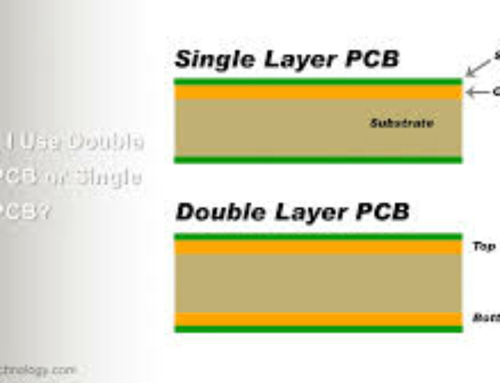
A PCB is a board used to mechanically support and electrically connect electronic components using conductive pathways, or traces, etched from copper sheets laminated onto a non-conductive substrate. While single layer PCBs have only one layer of conductive material, double layer PCBs, as the name suggests, have two layers of conductive material, typically copper, on both sides of the substrate.
The primary advantage of a double layer PCB over a single layer PCB is the increased complexity and density of the circuit that can be achieved.
This is particularly important in modern electronics, where space is often at a premium, and the need for more intricate and compact designs is ever-growing. By utilizing both sides of the board, designers can place more components and create more complex interconnections, thereby enhancing the functionality of the device without increasing its size.
Transitioning to the construction of a double layer PCB, it involves several key steps.
Initially, a substrate material, usually made of fiberglass-reinforced epoxy resin, is chosen for its insulating properties. Copper foil is then laminated onto both sides of this substrate. The next step involves applying a photosensitive resist to the copper layers, which is then exposed to ultraviolet light through a mask that defines the desired circuit pattern. The exposed resist hardens, while the unexposed areas remain soft and are subsequently washed away, revealing the copper beneath. This exposed copper is then etched away using a chemical solution, leaving behind the desired circuit traces. Finally, the hardened resist is removed, and the board undergoes a series of cleaning and finishing processes to prepare it for component assembly.
One of the critical aspects of double layer PCBs is the use of vias, which are small holes drilled through the board to allow electrical connections between the two layers.
These vias are typically filled with conductive material, such as copper, to ensure a reliable connection. The ability to connect traces on both sides of the board through vias significantly enhances the design flexibility and allows for more complex routing of electrical signals.
In terms of applications, double layer PCBs are ubiquitous in the electronics industry.
They are found in a wide range of devices, from consumer electronics like smartphones and laptops to industrial equipment and automotive systems. The versatility and efficiency of double layer PCBs make them an indispensable component in the development of modern electronic devices.
In conclusion, understanding the basics of double layer PCBs is essential for anyone involved in electronics design and manufacturing. These boards offer a significant advantage in terms of complexity and density, allowing for more compact and efficient designs. The construction process, involving the lamination of copper layers, application of resist, and etching, is intricate but crucial for creating reliable and functional circuits. The use of vias further enhances the design possibilities, making double layer PCBs a cornerstone of modern electronics. As technology continues to advance, the importance of double layer PCBs in enabling more sophisticated and compact devices will only continue to grow.
Advantages Of Using Double Layer PCBs In Modern Electronics
Double layer printed circuit boards (PCBs) have become a cornerstone in the realm of modern electronics, offering a multitude of advantages that cater to the ever-evolving demands of technology. These PCBs, characterized by having two conductive layers separated by an insulating substrate, provide a versatile platform for complex electronic designs.
One of the primary benefits of double layer PCBs is their ability to accommodate higher component density.
By utilizing both sides of the board for mounting components and routing traces, designers can create more intricate and compact circuits. This is particularly advantageous in applications where space is at a premium, such as in smartphones, wearable devices, and other portable electronics.
In addition to space efficiency, double layer PCBs enhance electrical performance.
The presence of two layers allows for more efficient routing of signals, reducing the length of traces and minimizing signal interference. This is crucial in high-speed and high-frequency applications where signal integrity is paramount. Furthermore, the ability to place ground and power planes on separate layers helps in reducing electromagnetic interference (EMI) and improving overall circuit stability.
This results in more reliable and robust electronic devices, which is essential in critical applications like medical equipment and aerospace technology.
Another significant advantage of double layer PCBs is their cost-effectiveness in medium to high-volume production. While single layer PCBs may be cheaper for very simple designs, the complexity and functionality required in modern electronics often necessitate the use of double layer boards.
The additional layer provides more routing options, which can lead to a reduction in the overall size of the PCB.
This, in turn, can lower material costs and reduce the need for additional interconnects, such as jumpers or connectors, which can be both costly and space-consuming. Moreover, the manufacturing processes for double layer PCBs have become highly optimized, making them a cost-effective solution for a wide range of applications.
The flexibility offered by double layer PCBs also extends to design modifications and iterations.
In the fast-paced world of electronics, the ability to quickly adapt and modify designs is invaluable. Double layer PCBs provide more routing options and design flexibility, allowing engineers to make changes without the need for a complete redesign. This can significantly shorten development cycles and bring products to market faster. Additionally, the use of computer-aided design (CAD) tools has made it easier to design and simulate double layer PCBs, further streamlining the development process.
Environmental considerations also play a role in the advantages of double layer PCBs.
With the growing emphasis on sustainability and reducing electronic waste, the ability to create more efficient and compact designs can lead to less material usage and lower energy consumption during manufacturing. This aligns with the broader goals of reducing the environmental impact of electronic devices and promoting more sustainable practices within the industry.
In conclusion, double layer PCBs offer a myriad of advantages that make them an indispensable component in modern electronics. Their ability to support higher component density, enhance electrical performance, provide cost-effective solutions, offer design flexibility, and contribute to environmental sustainability underscores their importance in the development of advanced electronic devices. As technology continues to advance, the role of double layer PCBs will undoubtedly remain pivotal in meeting the complex demands of contemporary electronic applications.
Design Considerations For Double Layer PCBs: Tips And Best Practices
When designing double layer printed circuit boards (PCBs), several critical considerations must be taken into account to ensure optimal performance and reliability. Double layer PCBs, which feature two conductive layers separated by an insulating substrate, offer increased complexity and functionality compared to single layer boards. However, this added complexity necessitates meticulous planning and adherence to best practices throughout the design process.
One of the primary considerations in double layer PCB design is the layout of the components and traces.
Proper component placement is crucial to minimize signal interference and ensure efficient routing. Components should be strategically positioned to reduce the length of critical signal paths, thereby minimizing potential signal degradation and electromagnetic interference (EMI). Additionally, placing components with similar functions in close proximity can simplify routing and enhance the overall organization of the PCB.
Transitioning to the routing of traces, it is essential to carefully plan the paths for signal and power traces.
Utilizing both layers effectively can help manage the complexity of the routing process. Signal traces should be routed on one layer, while the other layer can be dedicated to power and ground planes. This separation helps to reduce noise and improve signal integrity. Furthermore, employing a grid-based routing approach can aid in maintaining consistent trace widths and spacing, which is vital for ensuring reliable electrical performance.
Another important aspect to consider is the management of power distribution.
Ensuring a stable and efficient power supply to all components is paramount. To achieve this, designers should implement power planes or wide traces to distribute power evenly across the PCB. Additionally, decoupling capacitors should be placed near power pins of integrated circuits to filter out noise and provide a stable voltage supply. Proper grounding is equally important; a well-designed ground plane can significantly reduce EMI and improve overall signal integrity.
Thermal management is another critical factor in double layer PCB design.
As electronic components generate heat during operation, effective heat dissipation is necessary to prevent overheating and ensure longevity. Designers should consider the thermal properties of the materials used and incorporate thermal vias to facilitate heat transfer between layers. Additionally, placing heat-generating components away from heat-sensitive ones and using thermal relief pads can further enhance thermal management.
Signal integrity is a key consideration, particularly in high-speed applications.
To maintain signal integrity, designers should minimize the use of vias, as they can introduce impedance discontinuities and signal reflections. When vias are necessary, using blind or buried vias can help mitigate these issues. Additionally, maintaining consistent trace impedance by controlling trace width and spacing is crucial for high-speed signal transmission.
Design for manufacturability (DFM) is another essential consideration.
Ensuring that the PCB design can be efficiently and cost-effectively manufactured is vital for successful production. Designers should adhere to standard design rules and guidelines provided by PCB manufacturers, such as minimum trace width, spacing, and hole size. Additionally, incorporating test points and designing for ease of assembly can streamline the manufacturing process and reduce the likelihood of defects.
In conclusion, designing double layer PCBs requires careful consideration of various factors to achieve optimal performance and reliability. By strategically placing components, effectively routing traces, managing power distribution, addressing thermal management, maintaining signal integrity, and adhering to DFM principles, designers can create robust and efficient double layer PCBs. These best practices not only enhance the functionality of the PCB but also contribute to a smoother manufacturing process, ultimately leading to a successful end product.
Common Applications Of Double Layer PCBs In Various Industries
Double layer printed circuit boards (PCBs) are a fundamental component in modern electronics, offering a versatile and efficient solution for a wide range of applications across various industries. These PCBs, characterized by having two conductive layers of copper, enable more complex and compact circuit designs compared to single-layer PCBs. The additional layer allows for increased circuit density and improved electrical performance, making double layer PCBs a preferred choice in numerous sectors.
In the consumer electronics industry, double layer PCBs are extensively used due to their ability to support more intricate circuitry within compact devices.
Smartphones, tablets, and laptops are prime examples where these PCBs are indispensable. The dual-layer design facilitates the integration of multiple functionalities within a limited space, enhancing the overall performance and reliability of these gadgets. Moreover, the ability to route signals on both sides of the board reduces the need for additional wiring, contributing to the sleek and lightweight designs that consumers demand.
Transitioning to the automotive industry, double layer PCBs play a crucial role in the development of advanced vehicular systems.
Modern automobiles are equipped with a myriad of electronic components, from engine control units to infotainment systems, all of which rely on the robust and efficient design of double layer PCBs. These boards are essential for managing the complex electrical systems that ensure vehicle safety, performance, and comfort. For instance, the integration of sensors, control modules, and communication systems within a vehicle is made feasible through the use of double layer PCBs, which provide the necessary electrical pathways and support for these components.
In the realm of industrial automation, double layer PCBs are pivotal in the operation of machinery and control systems.
Industrial equipment often requires reliable and durable electronic circuits to manage processes and ensure precision. Double layer PCBs offer the necessary durability and flexibility to withstand harsh industrial environments while maintaining high performance. They are commonly found in programmable logic controllers (PLCs), motor drives, and other control systems that demand robust and efficient circuit designs. The ability to handle higher current loads and provide better heat dissipation further underscores their importance in industrial applications.
The medical industry also benefits significantly from the use of double layer PCBs.
Medical devices such as diagnostic equipment, monitoring systems, and therapeutic devices rely on the precision and reliability of these PCBs. The compact and efficient design of double layer PCBs allows for the development of portable and wearable medical devices, which are increasingly in demand for patient monitoring and home healthcare. Additionally, the stringent regulatory standards in the medical field necessitate the use of high-quality PCBs that can ensure consistent performance and safety, making double layer PCBs an ideal choice.
Furthermore, the telecommunications sector leverages double layer PCBs to support the infrastructure required for modern communication networks.
From base stations to routers and switches, these PCBs are integral in managing the complex signal processing and data transmission tasks. The ability to handle high-frequency signals and provide reliable connectivity is crucial in this industry, and double layer PCBs offer the necessary capabilities to meet these demands.
In conclusion, double layer PCBs are a versatile and essential component across various industries, enabling the development of advanced electronic systems. Their ability to support complex circuitry, improve electrical performance, and provide reliable operation makes them a cornerstone in the fields of consumer electronics, automotive, industrial automation, medical devices, and telecommunications. As technology continues to evolve, the demand for efficient and compact circuit solutions will only increase, further solidifying the importance of double layer PCBs in the modern technological landscape.