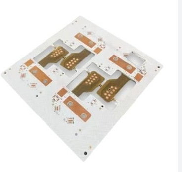
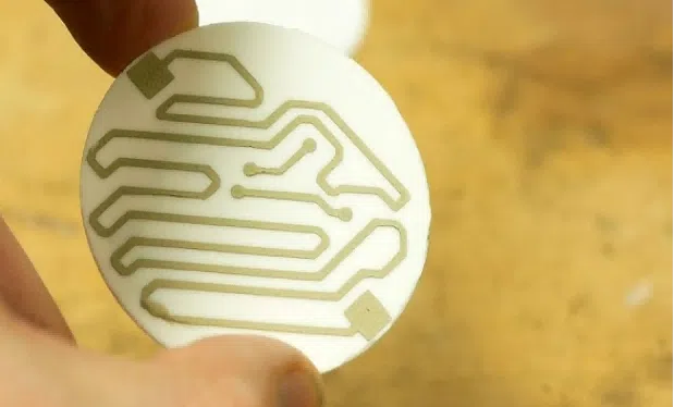
What is ceramic pcb
Introduction To Ceramic PCB: Understanding The Basics
Ceramic printed circuit boards (PCBs) represent a significant advancement in the field of electronic circuit design and manufacturing.
These specialized PCBs are constructed using ceramic materials, such as aluminum oxide (Al2O3), aluminum nitride (AlN), or beryllium oxide (BeO), which offer unique properties that make them highly suitable for specific applications.
To understand the basics of ceramic PCBs, it is essential to explore their composition, advantages, and typical uses in various industries.
Ceramic PCBs are distinguished from traditional PCBs by their substrate material.
While conventional PCBs typically use fiberglass-reinforced epoxy laminates, ceramic PCBs utilize ceramic substrates. This fundamental difference in material composition imparts several advantageous properties to ceramic PCBs. For instance, ceramic materials exhibit excellent thermal conductivity, which is crucial for dissipating heat generated by high-power electronic components. This thermal management capability ensures that the components operate within safe temperature ranges, thereby enhancing the reliability and longevity of the electronic device.
In addition to superior thermal performance, ceramic PCBs also offer exceptional electrical insulation properties.
The high dielectric strength of ceramic materials prevents electrical breakdown, even under high voltage conditions. This makes ceramic PCBs ideal for applications that require high voltage operation or where electrical isolation is paramount. Furthermore, ceramic substrates are inherently resistant to moisture and chemical corrosion, which contributes to the durability and stability of the PCB in harsh environments.
Another notable advantage of ceramic PCBs is their mechanical robustness.
Ceramic materials possess high mechanical strength and rigidity, which allows them to withstand mechanical stresses and vibrations without deforming or cracking. This characteristic is particularly beneficial in applications where the PCB is subjected to physical shocks or where structural integrity is critical. Moreover, the dimensional stability of ceramic substrates ensures that the PCB maintains its shape and size over a wide range of temperatures, further enhancing its reliability.
The unique properties of ceramic PCBs make them suitable for a variety of specialized applications.
In the aerospace and defense industries, for example, ceramic PCBs are used in radar systems, satellite communications, and missile guidance systems, where high performance and reliability are essential. In the automotive industry, ceramic PCBs are employed in engine control units, power modules, and sensors, where they must endure extreme temperatures and harsh operating conditions. Additionally, ceramic PCBs find applications in medical devices, such as implantable electronics and diagnostic equipment, where their biocompatibility and stability are critical.
Despite their numerous advantages, ceramic PCBs also present certain challenges.
The manufacturing process for ceramic PCBs is more complex and costly compared to traditional PCBs. The materials used are more expensive, and the fabrication techniques, such as thick-film and thin-film deposition, require specialized equipment and expertise. Consequently, the higher production costs may limit the widespread adoption of ceramic PCBs to applications where their unique properties are indispensable.
In conclusion, ceramic PCBs offer a range of benefits that make them highly suitable for specific high-performance and high-reliability applications. Their superior thermal conductivity, electrical insulation, mechanical strength, and environmental resistance set them apart from traditional PCBs. While the higher manufacturing costs may pose a challenge, the advantages of ceramic PCBs in critical applications cannot be overlooked. As technology continues to advance, the demand for ceramic PCBs is likely to grow, driven by the need for robust and reliable electronic solutions in increasingly demanding environments.
Advantages Of Using Ceramic PCBs In Modern Electronics
Ceramic printed circuit boards (PCBs) have emerged as a significant advancement in the field of modern electronics, offering a range of advantages that make them highly desirable for various applications.
One of the primary benefits of ceramic PCBs is their exceptional thermal conductivity.
Unlike traditional FR4 boards, ceramic substrates such as aluminum oxide (Al2O3) and aluminum nitride (AlN) can efficiently dissipate heat, which is crucial for high-power and high-frequency devices. This superior thermal management ensures that electronic components operate within safe temperature ranges, thereby enhancing their reliability and longevity.
In addition to thermal performance, ceramic PCBs exhibit excellent electrical insulation properties.
The inherent dielectric strength of ceramic materials minimizes the risk of electrical breakdown, making them suitable for high-voltage applications. This characteristic is particularly beneficial in industries such as aerospace, automotive, and telecommunications, where maintaining electrical integrity is paramount. Furthermore, the low dielectric constant of ceramic substrates reduces signal loss and crosstalk, thereby improving the overall performance of high-frequency circuits.
Another notable advantage of ceramic PCBs is their mechanical robustness.
Ceramic materials are inherently more rigid and durable compared to traditional PCB substrates. This mechanical strength allows ceramic PCBs to withstand harsh environmental conditions, including extreme temperatures, humidity, and mechanical stress. Consequently, they are ideal for use in demanding applications such as military and industrial electronics, where reliability and durability are critical.
Moreover, ceramic PCBs offer superior dimensional stability.
Unlike organic substrates that can expand or contract with temperature fluctuations, ceramic materials maintain their dimensions consistently. This stability is essential for precision applications, where even minor dimensional changes can affect the performance and alignment of electronic components. The dimensional stability of ceramic PCBs ensures that circuits remain accurate and reliable over time, contributing to the overall efficiency of electronic systems.
In terms of manufacturability, ceramic PCBs provide unique advantages as well.
Advanced manufacturing techniques such as Low-Temperature Co-fired Ceramic (LTCC) and High-Temperature Co-fired Ceramic (HTCC) allow for the integration of multiple layers and complex circuit designs. These techniques enable the creation of compact and high-density circuits, which are essential for modern electronic devices that demand miniaturization and high performance. Additionally, the ability to embed passive components such as resistors, capacitors, and inductors directly into the ceramic substrate further enhances the functionality and compactness of the final product.
Furthermore, ceramic PCBs are environmentally friendly.
The materials used in ceramic substrates are generally non-toxic and do not pose significant environmental hazards. This contrasts with some traditional PCB materials that may contain harmful substances. The eco-friendly nature of ceramic PCBs aligns with the growing emphasis on sustainability and environmental responsibility in the electronics industry.
In conclusion, the advantages of using ceramic PCBs in modern electronics are manifold. Their exceptional thermal conductivity, electrical insulation properties, mechanical robustness, dimensional stability, and advanced manufacturability make them an attractive choice for a wide range of applications. As the demand for high-performance, reliable, and compact electronic devices continues to grow, ceramic PCBs are poised to play an increasingly important role in the advancement of modern technology.
Manufacturing Process Of Ceramic PCBs: A Step-By-Step Guide
Ceramic printed circuit boards (PCBs) are increasingly becoming a preferred choice in various high-performance applications due to their superior thermal conductivity, mechanical strength, and electrical insulation properties. The manufacturing process of ceramic PCBs is intricate and involves several meticulous steps to ensure the final product meets the stringent requirements of modern electronic devices. This article provides a step-by-step guide to the manufacturing process of ceramic PCBs, elucidating the critical stages involved.
The journey begins with the selection of the ceramic substrate, which is typically made from materials such as alumina (Al2O3), aluminum nitride (AlN), or beryllium oxide (BeO).
These materials are chosen for their excellent thermal and electrical properties. Once the appropriate substrate is selected, it undergoes a thorough cleaning process to remove any contaminants that could affect the subsequent steps. This cleaning is usually performed using ultrasonic cleaning methods, ensuring the substrate is free from any particulate matter or residues.
Following the cleaning process, the next step involves the application of a conductive layer onto the ceramic substrate.
This is typically achieved through a process known as screen printing, where a conductive paste, often composed of silver, gold, or copper, is applied to the substrate in the desired circuit pattern. The screen printing process requires precision to ensure that the conductive paths are accurately formed. After the conductive paste is applied, the substrate is subjected to a drying process to remove any solvents present in the paste.
Subsequently, the dried substrate undergoes a firing process in a high-temperature furnace.
This step, known as sintering, is crucial as it solidifies the conductive paste, forming a robust and reliable conductive layer. The sintering temperature and duration are carefully controlled to optimize the electrical and mechanical properties of the conductive paths. Once the sintering process is complete, the substrate is allowed to cool gradually to prevent any thermal stress that could lead to cracks or warping.
The next phase involves the application of additional layers or components, depending on the complexity of the PCB design.
For multilayer ceramic PCBs, multiple layers of ceramic and conductive materials are alternately stacked and bonded together. This stacking process requires precise alignment to ensure that the vias, or vertical interconnections between layers, are accurately positioned. The stacked layers are then subjected to another sintering process to bond them into a single, cohesive unit.
After the multilayer structure is formed, the PCB undergoes a series of inspection and testing procedures to ensure its integrity and functionality.
These inspections include visual checks for any defects, as well as electrical testing to verify the continuity and resistance of the conductive paths. Advanced testing methods, such as X-ray inspection, may also be employed to detect any hidden defects within the multilayer structure.
Finally, the ceramic PCB is ready for the finishing touches, which may include the application of protective coatings, solder masks, or surface finishes to enhance its durability and performance. The finished PCB is then subjected to a final round of quality control checks before being packaged and shipped to the customer.
In conclusion, the manufacturing process of ceramic PCBs is a complex and precise endeavor that involves multiple stages, from substrate preparation to final inspection. Each step is critical in ensuring that the final product meets the high standards required for advanced electronic applications. By understanding this process, one can appreciate the meticulous craftsmanship and technological expertise that go into producing these high-performance circuit boards.

Applications Of Ceramic PCBs In Various Industries
Ceramic printed circuit boards (PCBs) have emerged as a pivotal technology in various industries due to their unique properties and advantages over traditional PCB materials. These boards are primarily composed of ceramic substrates such as aluminum oxide (Al2O3), aluminum nitride (AlN), and beryllium oxide (BeO), which offer superior thermal conductivity, electrical insulation, and mechanical strength. Consequently, ceramic PCBs are increasingly being adopted in applications where these characteristics are critical.
One of the primary industries benefiting from ceramic PCBs is the aerospace sector.
In this field, the ability to withstand extreme temperatures and harsh environmental conditions is paramount. Ceramic PCBs excel in these areas, providing reliable performance in high-altitude and space environments where traditional PCBs might fail. Their high thermal conductivity ensures efficient heat dissipation, which is crucial for maintaining the integrity of electronic components in aerospace applications.
Similarly, the automotive industry has found ceramic PCBs to be indispensable, particularly in the development of electric vehicles (EVs) and advanced driver-assistance systems (ADAS).
The high power density and thermal management capabilities of ceramic PCBs make them ideal for use in power electronics, battery management systems, and other critical components of EVs. Additionally, their robustness and reliability enhance the safety and performance of ADAS, which are essential for modern vehicles.
In the realm of telecommunications, ceramic PCBs play a vital role in the development of high-frequency and high-power devices.
The low dielectric loss and high thermal conductivity of ceramic substrates enable the efficient transmission of signals with minimal interference, making them suitable for use in radio frequency (RF) and microwave applications. This is particularly important in the deployment of 5G technology, where the demand for high-speed data transmission and low latency is ever-increasing.
The medical industry also leverages the advantages of ceramic PCBs, particularly in the design and manufacture of medical devices and equipment.
The biocompatibility and stability of ceramic materials make them suitable for use in implantable devices, such as pacemakers and neurostimulators. Furthermore, the high thermal conductivity and electrical insulation properties of ceramic PCBs ensure the reliable operation of diagnostic equipment, such as MRI machines and ultrasound devices, which require precise and stable electronic performance.
In the field of industrial automation, ceramic PCBs are utilized in the development of high-power and high-temperature applications.
The durability and thermal management capabilities of ceramic substrates make them ideal for use in power modules, motor drives, and other industrial control systems. These applications often operate in demanding environments, where the reliability and longevity of electronic components are critical to maintaining operational efficiency and reducing downtime.
Moreover, the lighting industry has embraced ceramic PCBs, particularly in the production of high-power LED lighting systems.
The excellent thermal conductivity of ceramic substrates allows for efficient heat dissipation, which is essential for maintaining the performance and lifespan of LEDs. This is especially important in applications such as street lighting, automotive lighting, and high-intensity industrial lighting, where consistent and reliable illumination is required.
In conclusion, the unique properties of ceramic PCBs have made them an invaluable component across a wide range of industries. Their superior thermal conductivity, electrical insulation, and mechanical strength enable them to meet the demanding requirements of aerospace, automotive, telecommunications, medical, industrial automation, and lighting applications. As technology continues to advance, the adoption of ceramic PCBs is likely to expand further, driving innovation and enhancing the performance and reliability of electronic systems in various sectors.