USB 3.0 pcb design guide
Key Considerations for USB 3.0 PCB Layout
When designing a printed circuit board (PCB) for USB 3.0, several key considerations must be taken into account to ensure optimal performance and reliability. USB 3.0, also known as SuperSpeed USB, offers significant improvements over its predecessors, including higher data transfer rates of up to 5 Gbps. To achieve these speeds, meticulous attention to detail in the PCB layout is essential.
Firstly, signal integrity is paramount in USB 3.0 PCB design.
High-speed signals are susceptible to various forms of interference and degradation, which can lead to data errors and reduced performance. To mitigate these issues, it is crucial to maintain controlled impedance for the differential pairs. This involves carefully designing the trace width, spacing, and the dielectric material of the PCB. Differential pairs should be routed with consistent spacing and minimal skew to ensure that the signals arrive simultaneously at the receiver.
Moreover, minimizing crosstalk is another critical aspect.
Crosstalk occurs when signals on adjacent traces interfere with each other, which can be particularly problematic at high frequencies. To reduce crosstalk, it is advisable to maintain adequate spacing between high-speed traces and to use ground planes effectively. Ground planes not only provide a return path for signals but also act as a shield to reduce electromagnetic interference (EMI).
In addition to signal integrity, power integrity must also be considered.
USB 3.0 devices often require significant power, and any fluctuations in the power supply can affect performance. To ensure stable power delivery, it is important to use decoupling capacitors close to the power pins of the USB controller and other critical components. These capacitors help to filter out noise and provide a stable voltage. Additionally, using wide power and ground traces can reduce the impedance and improve the overall power distribution network.
Thermal management is another key consideration in USB 3.0 PCB design.
High-speed data transfer can generate significant heat, which needs to be dissipated effectively to prevent overheating and potential damage to components. Proper thermal management can be achieved by using thermal vias, heat sinks, and ensuring adequate airflow around the PCB. Thermal vias help to transfer heat from the surface of the PCB to the inner layers or to an external heat sink, thereby improving heat dissipation.
Furthermore, the placement of components plays a crucial role in the overall performance of the USB 3.0 PCB.
Critical components such as the USB controller, connectors, and power management ICs should be placed strategically to minimize the length of high-speed traces and reduce potential signal degradation. It is also important to avoid placing high-speed traces near noisy components such as switching regulators or oscillators, as this can introduce unwanted interference.
Lastly, compliance with USB 3.0 specifications and standards is essential.
Adhering to these standards ensures that the PCB design will be compatible with other USB 3.0 devices and will perform reliably under various conditions. This includes following guidelines for trace impedance, differential pair routing, and connector placement. Additionally, thorough testing and validation of the PCB design are necessary to identify and address any potential issues before mass production.
In conclusion, designing a PCB for USB 3.0 requires careful consideration of signal integrity, power integrity, thermal management, component placement, and compliance with standards. By addressing these key factors, designers can create a robust and reliable PCB that takes full advantage of the high-speed capabilities of USB 3.0 technology.
Signal Integrity in USB 3.0 PCB Design
Signal integrity is a critical consideration in the design of USB 3.0 printed circuit boards (PCBs). As USB 3.0 technology supports data transfer rates up to 5 Gbps, maintaining signal integrity becomes paramount to ensure reliable communication between devices. To achieve this, designers must pay close attention to various factors, including trace impedance, crosstalk, and electromagnetic interference (EMI).
One of the primary aspects to consider is the characteristic impedance of the traces.
For USB 3.0, the differential pair impedance should be maintained at 90 ohms. This requires careful control of trace width, spacing, and the dielectric properties of the PCB material. Deviations from the specified impedance can result in signal reflections, which degrade the signal quality and potentially lead to data errors. Therefore, it is essential to use precise PCB fabrication techniques and tools to ensure that the impedance remains within the acceptable range.
In addition to impedance control, minimizing crosstalk is crucial for maintaining signal integrity.
Crosstalk occurs when a signal transmitted on one trace induces an unwanted signal on an adjacent trace. This can be particularly problematic in high-speed designs like USB 3.0, where even small amounts of crosstalk can significantly impact performance. To mitigate crosstalk, designers should maintain adequate spacing between high-speed differential pairs and other signal traces. Furthermore, employing ground planes and proper layer stacking can help to isolate signals and reduce the potential for crosstalk.
Electromagnetic interference (EMI) is another significant concern in USB 3.0 PCB design.
EMI can originate from various sources, including other electronic components and external devices. To minimize EMI, designers should implement proper shielding techniques and use high-quality components. Additionally, ensuring that the PCB layout follows best practices for high-speed design can help to reduce EMI. For instance, keeping trace lengths as short as possible and avoiding sharp bends can minimize the potential for EMI.
Moreover, the use of differential signaling in USB 3.0 helps to enhance signal integrity by reducing susceptibility to external noise.
Differential pairs transmit the same signal on two traces with opposite polarities, which allows the receiver to cancel out any common-mode noise. However, for differential signaling to be effective, it is essential to maintain symmetry between the traces. This includes ensuring equal trace lengths and consistent spacing throughout the PCB layout.
Power integrity is also a vital aspect of maintaining signal integrity in USB 3.0 designs.
Stable power delivery is necessary to ensure that the transceivers and other components function correctly. Designers should use decoupling capacitors strategically placed near power pins to filter out noise and provide a stable power supply. Additionally, using a solid ground plane can help to reduce ground bounce and improve overall power integrity.
Thermal management is another factor that can influence signal integrity.
High-speed data transmission generates heat, which can affect the performance of the PCB and its components. Proper thermal management techniques, such as using thermal vias and heat sinks, can help to dissipate heat and maintain optimal operating conditions.
In conclusion, maintaining signal integrity in USB 3.0 PCB design requires a comprehensive approach that addresses impedance control, crosstalk reduction, EMI mitigation, differential signaling, power integrity, and thermal management. By carefully considering these factors and following best practices for high-speed PCB design, engineers can ensure reliable and efficient performance of USB 3.0 devices.
Power Delivery and Grounding Strategies for USB 3.0 PCBs
In the realm of USB 3.0 PCB design, power delivery and grounding strategies are paramount to ensuring optimal performance and reliability. The USB 3.0 standard, with its increased data transfer rates and enhanced power capabilities, necessitates meticulous attention to these aspects. Effective power delivery and grounding are critical not only for maintaining signal integrity but also for minimizing electromagnetic interference (EMI) and ensuring the overall stability of the system.
To begin with, power delivery in USB 3.0 PCBs must be designed to handle the higher current requirements associated with the standard.
USB 3.0 can deliver up to 900mA of current, compared to the 500mA provided by USB 2.0. This increase necessitates the use of wider power traces to reduce resistive losses and ensure efficient power distribution. It is advisable to use multiple power planes or a dedicated power layer in the PCB stack-up to provide a low-impedance path for the current. This approach not only enhances power delivery but also helps in reducing voltage drops across the PCB.
Transitioning to grounding strategies, a solid and continuous ground plane is essential for USB 3.0 PCBs.
The ground plane serves as a reference point for all signals and helps in maintaining signal integrity by providing a low-impedance return path for the current. A well-designed ground plane minimizes the loop area, thereby reducing the potential for EMI. It is crucial to avoid splitting the ground plane, as discontinuities can lead to increased noise and signal degradation. If multiple ground planes are used, they should be connected through numerous vias to ensure a low-impedance connection.
Moreover, the placement of decoupling capacitors plays a significant role in power delivery and grounding.
Decoupling capacitors should be placed as close as possible to the power pins of the USB 3.0 components. These capacitors help in filtering out high-frequency noise and provide a stable power supply to the components. It is recommended to use a combination of capacitors with different values to cover a wide range of frequencies. For instance, using a mix of 0.1µF, 1µF, and 10µF capacitors can effectively filter out noise across various frequency bands.
In addition to decoupling capacitors, the use of ferrite beads can further enhance power integrity.
Ferrite beads act as low-pass filters, attenuating high-frequency noise while allowing DC signals to pass through. Placing ferrite beads in series with the power supply lines can help in reducing EMI and improving the overall performance of the USB 3.0 PCB.
Another critical aspect of grounding is the implementation of proper shielding techniques.
Shielding can be achieved by enclosing the USB 3.0 traces in a grounded metal enclosure or by using ground traces adjacent to the signal traces. This approach helps in containing the electromagnetic fields and preventing them from radiating outwards. Additionally, differential pairs, which are commonly used in USB 3.0 for high-speed data transmission, should be routed with controlled impedance and proper spacing to minimize crosstalk and signal degradation.
In conclusion, power delivery and grounding strategies are integral to the design of USB 3.0 PCBs. By employing wider power traces, maintaining a solid ground plane, strategically placing decoupling capacitors, using ferrite beads, and implementing effective shielding techniques, designers can ensure the reliable operation of USB 3.0 devices. These practices not only enhance signal integrity and reduce EMI but also contribute to the overall robustness and performance of the system.
Best Practices for USB 3.0 Differential Pair Routing
When designing a printed circuit board (PCB) for USB 3.0, one of the most critical aspects to consider is the routing of differential pairs. USB 3.0, with its high data transfer rates of up to 5 Gbps, demands meticulous attention to detail to ensure signal integrity and minimize electromagnetic interference (EMI). Adhering to best practices for differential pair routing is essential to achieve optimal performance and reliability.
To begin with, it is crucial to maintain the differential pairs’ impedance.
USB 3.0 differential pairs typically require a differential impedance of 90 ohms. This can be achieved by carefully selecting the trace width and spacing, as well as the PCB stack-up. Consistency in these parameters is vital; any variation can lead to impedance mismatches, which can degrade signal quality. Utilizing impedance calculators or simulation tools can aid in achieving the desired impedance.
Another important consideration is the length matching of the differential pairs.
USB 3.0 signals are highly sensitive to timing differences, and any length mismatch can result in skew, leading to data errors. It is recommended to keep the length difference between the two traces of a differential pair to within 5 mils (0.127 mm). This can be accomplished by using serpentine routing or meandering techniques to equalize the lengths.
In addition to length matching, it is essential to maintain a consistent spacing between the differential pairs.
The spacing should be kept as uniform as possible to avoid impedance discontinuities. Furthermore, differential pairs should be routed as close together as possible to maximize coupling and minimize noise susceptibility. This close coupling helps to ensure that any external noise affects both traces equally, thereby preserving the differential signal integrity.
When routing differential pairs, it is also important to avoid sharp bends.
Sharp corners can cause impedance discontinuities and signal reflections, which can degrade signal quality. Instead, use gentle curves or 45-degree angles to route the traces. This practice helps to maintain a consistent impedance and reduces the risk of signal degradation.
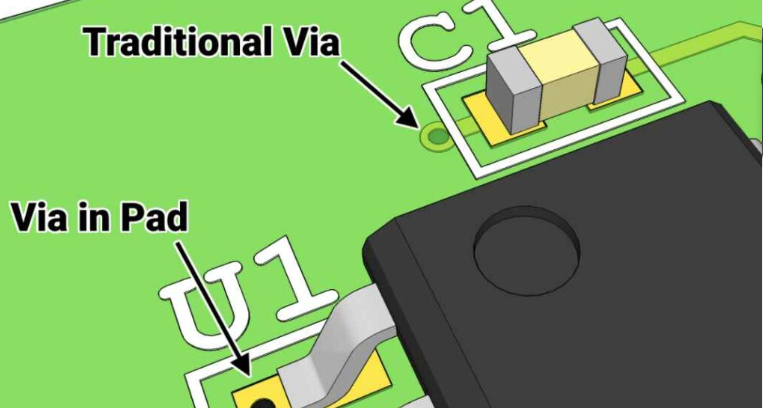
Ground planes play a significant role in differential pair routing.
A continuous ground plane beneath the differential pairs provides a return path for the signals and helps to minimize EMI. It is advisable to avoid routing differential pairs over split ground planes or across gaps in the ground plane, as this can lead to impedance discontinuities and increased EMI. Additionally, placing ground vias near the differential pairs can further enhance signal integrity by providing a low-impedance return path.
Crosstalk is another critical factor to consider in USB 3.0 differential pair routing.
To minimize crosstalk, it is important to maintain adequate spacing between adjacent differential pairs and other high-speed signals. A general rule of thumb is to keep a spacing of at least three times the trace width between differential pairs and other signals. This helps to reduce the risk of crosstalk and ensures signal integrity.
Finally, it is essential to perform thorough signal integrity analysis and testing.
Simulation tools can be used to model the PCB and predict potential issues with differential pair routing. Once the PCB is fabricated, it is important to conduct signal integrity testing to verify that the differential pairs meet the required performance specifications.
In conclusion, following best practices for USB 3.0 differential pair routing is crucial to achieving high signal integrity and reliable performance. By maintaining consistent impedance, length matching, and spacing, avoiding sharp bends, ensuring a continuous ground plane, minimizing crosstalk, and conducting thorough testing, designers can optimize their PCB designs for USB 3.0 applications.